- lides topic

Содержание
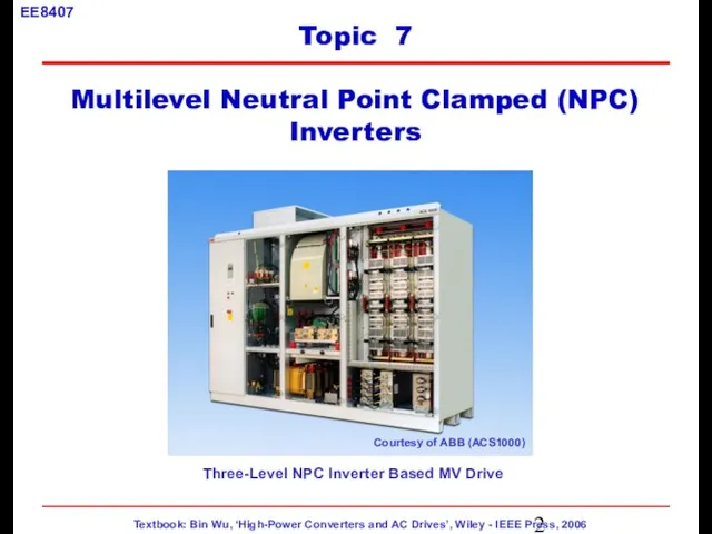
- 2. Three-Level NPC Inverter Based MV Drive Topic 7 Multilevel Neutral Point Clamped (NPC) Inverters Courtesy of
- 3. Lecture Topics Three-level NPC Inverter Space Vector Modulation Neutral Point Voltage Control High-level NPC Inverters Multilevel
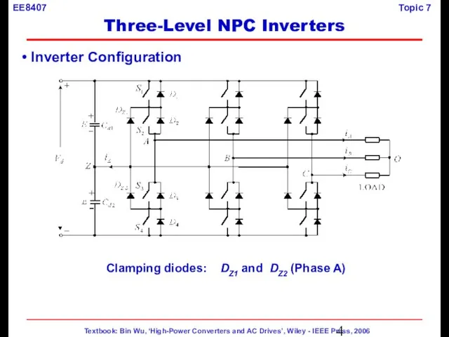
- 4. Inverter Configuration Clamping diodes: DZ1 and DZ2 (Phase A) Three-Level NPC Inverters
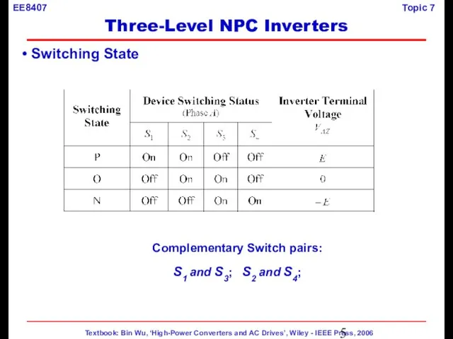
- 5. Switching State Complementary Switch pairs: S1 and S3; S2 and S4; Three-Level NPC Inverters
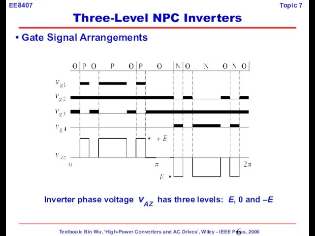
- 6. Gate Signal Arrangements Inverter phase voltage vAZ has three levels: E, 0 and –E Three-Level NPC
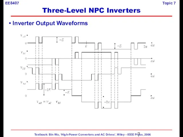
- 7. Inverter Output Waveforms Three-Level NPC Inverters
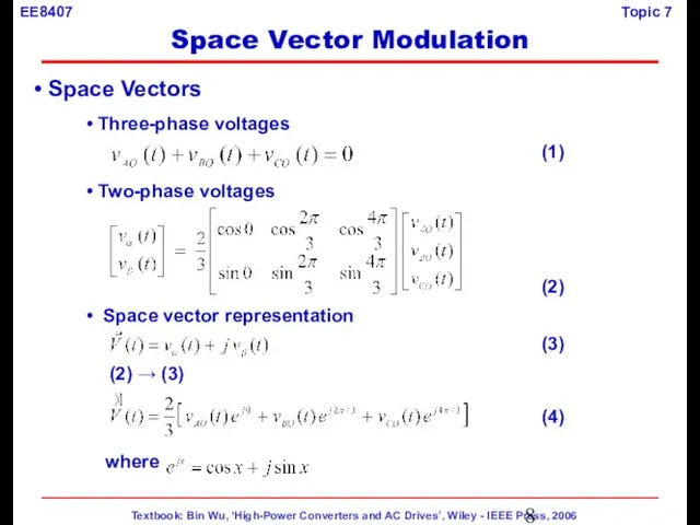
- 8. Space Vectors Three-phase voltages Two-phase voltages Space vector representation (2) → (3) where (3) (1) (2)
- 9. Switching state [POO] → on-state switches: Phase A: upper two switches [P] Phase B: middle two
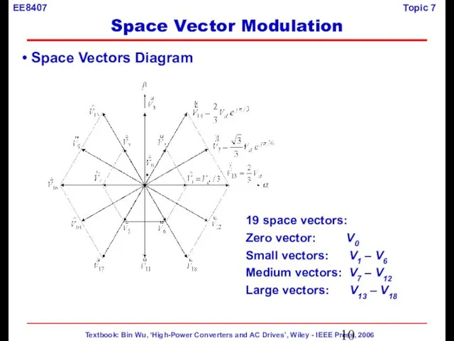
- 10. Space Vectors Diagram 19 space vectors: Zero vector: V0 Small vectors: V1 – V6 Medium vectors:
- 11. Switching States and Space Vectors Redundancy: Zero vector – three switching states Small vectors – two
- 12. No redundant switching states for medium or large vectors Switching States and Space Vectors Space Vector
- 13. Sector Definition Vref : Reference vector, rotating in space at a certain speed; All other vectors
- 14. SVM Principle For a given length and position in space, Vref can be approximated by three
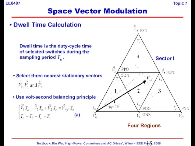
- 15. Dwell Time Calculation Use volt-second balancing principle Select three nearest stationary vectors Sector I Four Regions
- 16. Dwell Time Calculation Ta , Tb and Tc – dwell times for V1 , V7 and
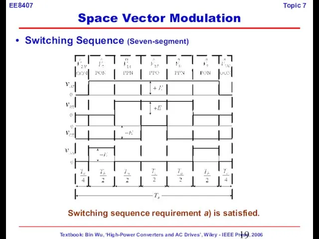
- 17. Switching Sequence (Seven-segment) General Design Requirements a) The transition from one switching state to the next
- 18. Switching Sequence (Seven-segment) Assuming Vref is in Region 4 of Sector I, three vectors are selected:
- 19. Switching Sequence (Seven-segment) Switching sequence requirement a) is satisfied. Space Vector Modulation
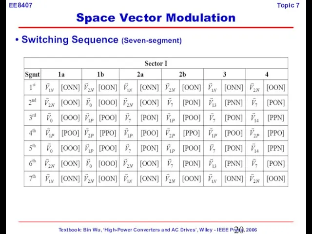
- 20. Switching Sequence (Seven-segment) Space Vector Modulation
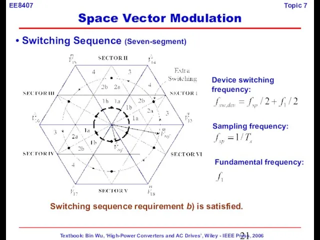
- 21. Switching Sequence (Seven-segment) Switching sequence requirement b) is satisfied. Device switching frequency: Sampling frequency: Fundamental frequency:
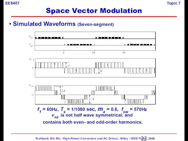
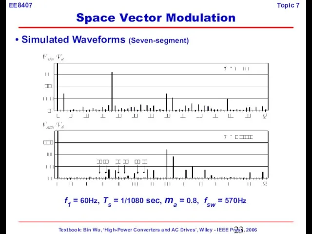
- 22. Simulated Waveforms (Seven-segment) f1 = 60Hz, Ts = 1/1080 sec, ma = 0.8, fsw = 570Hz
- 23. Simulated Waveforms (Seven-segment) f1 = 60Hz, Ts = 1/1080 sec, ma = 0.8, fsw = 570Hz
- 24. Harmonic Content (Seven-segment) Space Vector Modulation
- 25. Laboratory Prototype at Ryerson Space Vector Modulation
- 26. Measured Waveforms Space Vector Modulation
- 27. Measured waveforms (with even-order harmonic elimination) Space Vector Modulation
- 28. Neutral Point Voltage Deviation The neutral point voltage vz can be controlled by P- and N-types
- 29. Neutral Point Voltage Control Neutral Point Voltage Control
- 30. Neutral Point Voltage Control R is used on purpose to make the dc voltage unbalance. Neutral
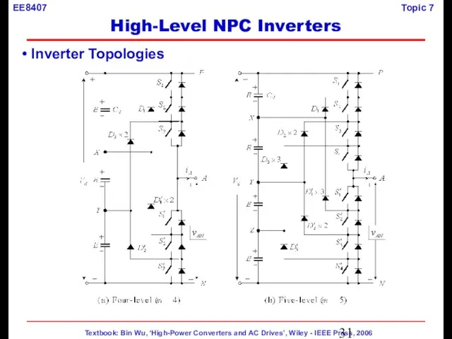
- 31. Inverter Topologies High-Level NPC Inverters
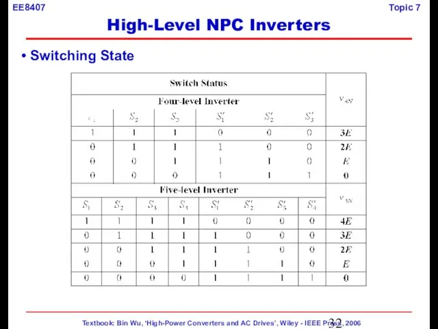
- 32. Switching State High-Level NPC Inverters
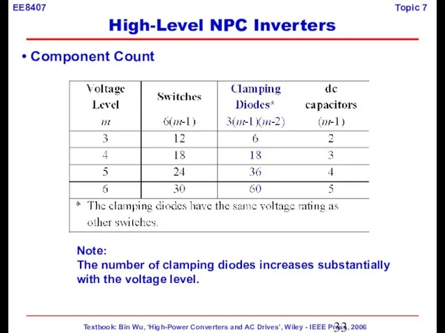
- 33. Component Count Note: The number of clamping diodes increases substantially with the voltage level. High-Level NPC
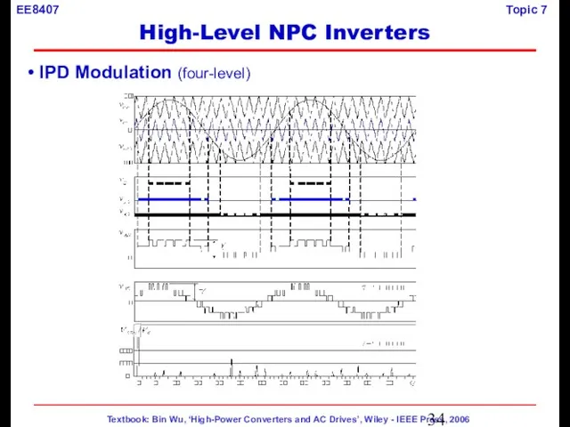
- 34. IPD Modulation (four-level) High-Level NPC Inverters
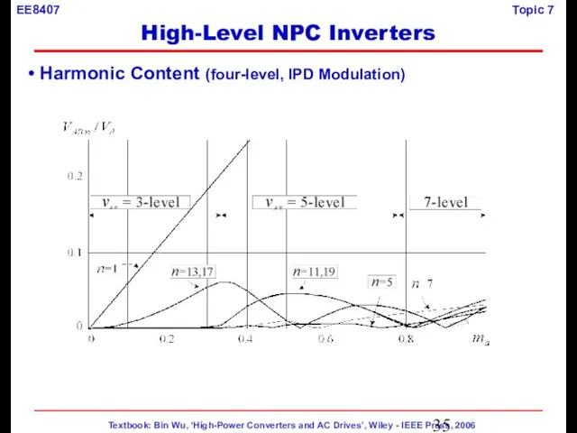
- 35. Harmonic Content (four-level, IPD Modulation) High-Level NPC Inverters
- 36. APOD Modulation (four-level) High-Level NPC Inverters
- 37. Harmonic Content (four-level, APOD Modulation) High-Level NPC Inverters
- 38. The 3-level NPC inverter widely used in MV drives Main features - Low device count -
- 40. Скачать презентацию
Слайд 2Three-Level NPC Inverter Based MV Drive
Topic 7
Multilevel Neutral Point Clamped (NPC)
Inverters
Courtesy
Three-Level NPC Inverter Based MV Drive
Topic 7
Multilevel Neutral Point Clamped (NPC)
Inverters
Courtesy
Слайд 3 Lecture Topics
Three-level NPC Inverter
Space Vector Modulation
Neutral Point Voltage Control
Lecture Topics
Three-level NPC Inverter
Space Vector Modulation
Neutral Point Voltage Control
Слайд 4 Inverter Configuration
Clamping diodes: DZ1 and DZ2 (Phase A)
Three-Level NPC Inverters
Inverter Configuration
Clamping diodes: DZ1 and DZ2 (Phase A)
Three-Level NPC Inverters
Слайд 5 Switching State
Complementary Switch pairs:
S1 and S3; S2 and S4;
Three-Level NPC
Switching State
Complementary Switch pairs:
S1 and S3; S2 and S4;
Three-Level NPC
Слайд 6 Gate Signal Arrangements
Inverter phase voltage vAZ has three levels: E, 0
Gate Signal Arrangements
Inverter phase voltage vAZ has three levels: E, 0
Слайд 7 Inverter Output Waveforms
Three-Level NPC Inverters
Inverter Output Waveforms
Three-Level NPC Inverters
Слайд 8 Space Vectors
Three-phase voltages
Two-phase voltages
Space vector representation
(2) → (3)
Space Vectors
Three-phase voltages
Two-phase voltages
Space vector representation
(2) → (3)
Слайд 9Switching state [POO] → on-state switches:
Phase A: upper two switches [P]
Phase B:
Switching state [POO] → on-state switches:
Phase A: upper two switches [P]
Phase B:
![Switching state [POO] → on-state switches: Phase A: upper two switches [P]](/_ipx/f_webp&q_80&fit_contain&s_1440x1080/imagesDir/jpg/381591/slide-8.jpg)
Слайд 10 Space Vectors Diagram
19 space vectors:
Zero vector: V0
Small vectors: V1 –
Space Vectors Diagram
19 space vectors:
Zero vector: V0
Small vectors: V1 –
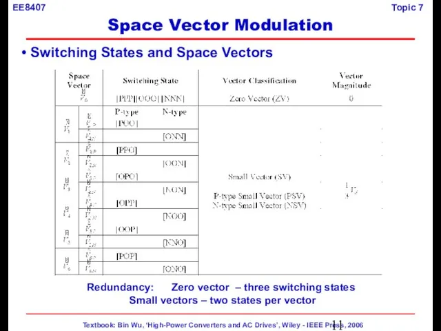
Слайд 11 Switching States and Space Vectors
Redundancy: Zero vector – three switching
Switching States and Space Vectors
Redundancy: Zero vector – three switching
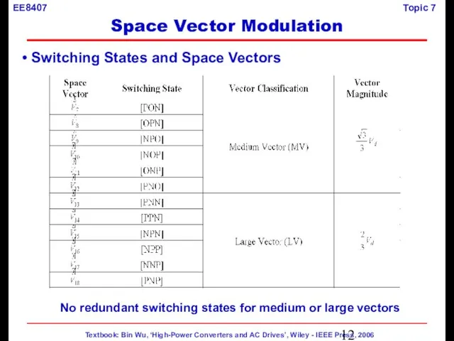
Слайд 12No redundant switching states for medium or large vectors
Switching States and
No redundant switching states for medium or large vectors
Switching States and
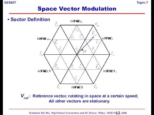
Слайд 13 Sector Definition
Vref : Reference vector, rotating in space at a
Sector Definition
Vref : Reference vector, rotating in space at a
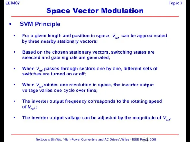
Слайд 14 SVM Principle
For a given length and position in space, Vref
SVM Principle
For a given length and position in space, Vref
Слайд 15 Dwell Time Calculation
Use volt-second balancing principle
Select three nearest
Dwell Time Calculation
Use volt-second balancing principle
Select three nearest
Слайд 16 Dwell Time Calculation
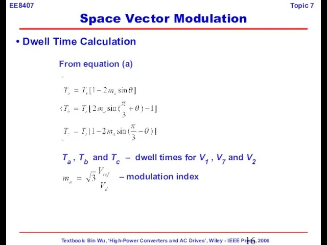
Ta , Tb and Tc – dwell times
Dwell Time Calculation
Ta , Tb and Tc – dwell times
Слайд 17 Switching Sequence (Seven-segment)
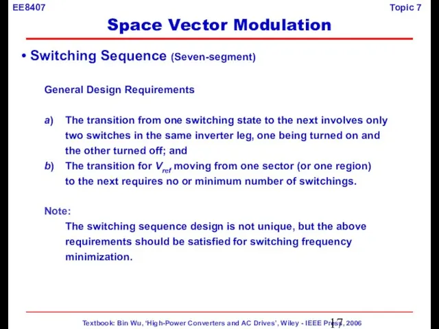
General Design Requirements
a) The transition from one switching
Switching Sequence (Seven-segment)
General Design Requirements
a) The transition from one switching
Слайд 18 Switching Sequence (Seven-segment)
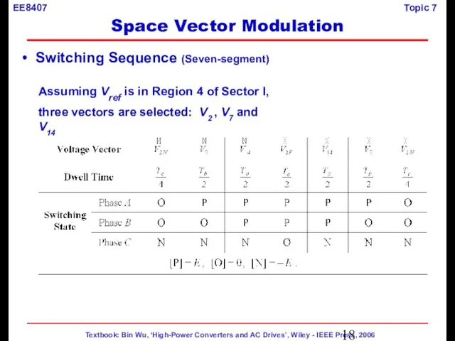
Assuming Vref is in Region 4 of Sector
Switching Sequence (Seven-segment)
Assuming Vref is in Region 4 of Sector
Слайд 19 Switching Sequence (Seven-segment)
Switching sequence requirement a) is satisfied.
Space Vector Modulation
Switching Sequence (Seven-segment)
Switching sequence requirement a) is satisfied.
Space Vector Modulation
Слайд 20 Switching Sequence (Seven-segment)
Space Vector Modulation
Switching Sequence (Seven-segment)
Space Vector Modulation
Слайд 21 Switching Sequence (Seven-segment)
Switching sequence requirement b) is satisfied.
Device switching frequency:
Sampling
Switching Sequence (Seven-segment)
Switching sequence requirement b) is satisfied.
Device switching frequency:
Sampling
Слайд 22 Simulated Waveforms (Seven-segment)
f1 = 60Hz, Ts = 1/1080 sec, ma
Simulated Waveforms (Seven-segment)
f1 = 60Hz, Ts = 1/1080 sec, ma
Слайд 23 Simulated Waveforms (Seven-segment)
f1 = 60Hz, Ts = 1/1080 sec, ma
Simulated Waveforms (Seven-segment)
f1 = 60Hz, Ts = 1/1080 sec, ma
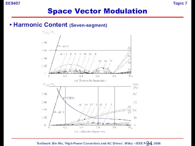
Слайд 24 Harmonic Content (Seven-segment)
Space Vector Modulation
Harmonic Content (Seven-segment)
Space Vector Modulation
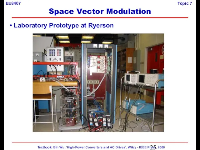
Слайд 25 Laboratory Prototype at Ryerson
Space Vector Modulation
Laboratory Prototype at Ryerson
Space Vector Modulation
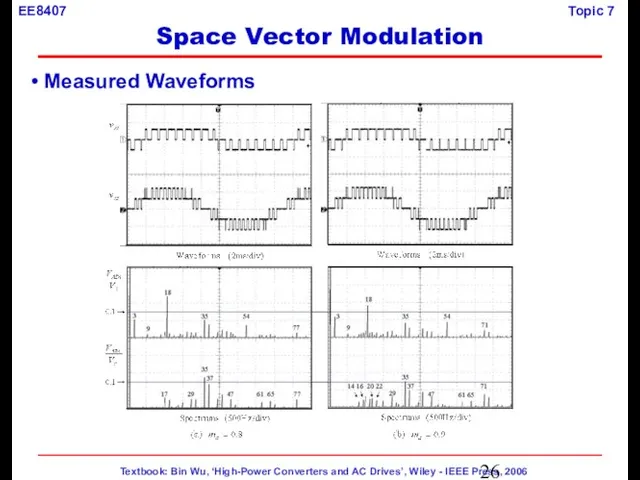
Слайд 26 Measured Waveforms
Space Vector Modulation
Measured Waveforms
Space Vector Modulation
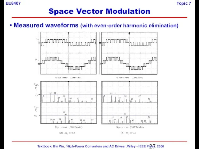
Слайд 27 Measured waveforms (with even-order harmonic elimination)
Space Vector Modulation
Measured waveforms (with even-order harmonic elimination)
Space Vector Modulation
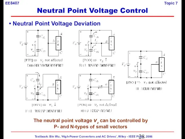
Слайд 28 Neutral Point Voltage Deviation
The neutral point voltage vz can be controlled
Neutral Point Voltage Deviation
The neutral point voltage vz can be controlled
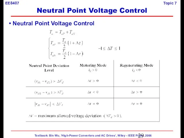
Слайд 29 Neutral Point Voltage Control
Neutral Point Voltage Control
Neutral Point Voltage Control
Neutral Point Voltage Control
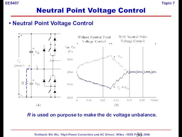
Слайд 30 Neutral Point Voltage Control
R is used on purpose to make
Neutral Point Voltage Control
R is used on purpose to make
Слайд 31 Inverter Topologies
High-Level NPC Inverters
Inverter Topologies
High-Level NPC Inverters
Слайд 32 Switching State
High-Level NPC Inverters
Switching State
High-Level NPC Inverters
Слайд 33 Component Count
Note:
The number of clamping diodes increases substantially
with the
Component Count
Note:
The number of clamping diodes increases substantially
with the
Слайд 34 IPD Modulation (four-level)
High-Level NPC Inverters
IPD Modulation (four-level)
High-Level NPC Inverters
Слайд 35 Harmonic Content (four-level, IPD Modulation)
High-Level NPC Inverters
Harmonic Content (four-level, IPD Modulation)
High-Level NPC Inverters
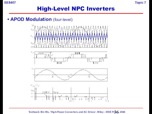
Слайд 36 APOD Modulation (four-level)
High-Level NPC Inverters
APOD Modulation (four-level)
High-Level NPC Inverters
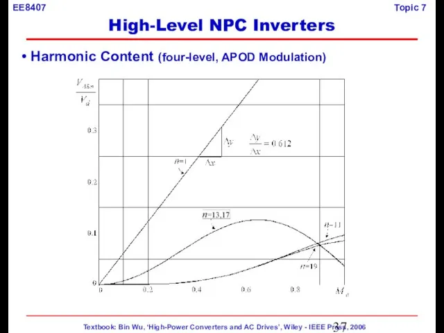
Слайд 37 Harmonic Content (four-level, APOD Modulation)
High-Level NPC Inverters
Harmonic Content (four-level, APOD Modulation)
High-Level NPC Inverters
Слайд 38
The 3-level NPC inverter widely used in MV drives
Main
The 3-level NPC inverter widely used in MV drives
Main
 Негативное влияние шума на здоровье человека
 Рисунки Беловой Э.Ю
 Правила написания эссе
 Ыдык байырлалывыс – ынак Шагаавыс
 Желание бросить - Мотивация: Важная роль лечащего врача
 Работа с программой WS Movie Maker
 Развитие личности школьника (1 – 7 класс)
 Программа направлена на усиление академической мобильности студентов и преподавателей, укрепление сотрудничества университетов
 Алексей Николаевич Толстой
 Какую роль играют комнатные растения в жизни человека
 Основы административного права
 Хохломская роспись и компьютерная графика
 ЗВІТ голови Ширяївської районної державної адміністрації Одеської області за період 10.09.2015 р. – 16.01.2017 р
 Звук
Звук Кришна (Верховная Личность Бога)
 Богемское стекло
 Презентация на тему Юго-Восточная Азия
 Презентация на тему Полуфабрикаты из мяса
  Системы развития подростков: сервисы, курсы, консалтинг, сообщества
 Программы поддержки международных проектов в области культуры и просвещения Витаут Рудник, общественное объединение «Центр «Тре
 Урок 32
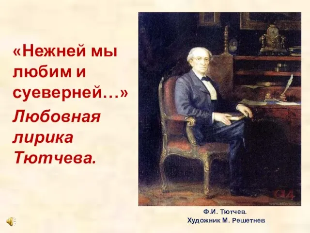 Презентация на тему Любовная лирика Тютчева
 Использование ИКТ в учебном процессе
 Наруто и Хината
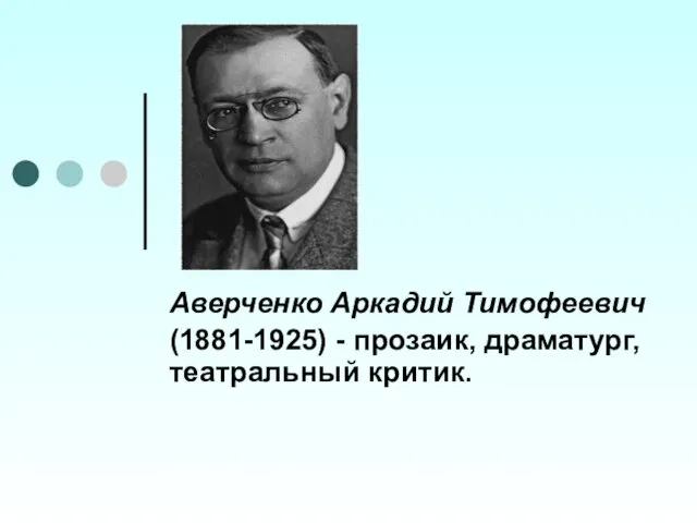 Аверченко Аркадий Тимофеевич
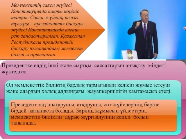 Мемлекеттің саяси жүйесі Конституцияда нақты көрініс тапқан
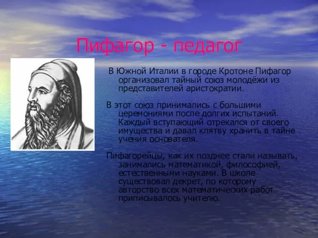 Пифагор - педагог
 10. Интонация предложения