- Plasma Etching

Содержание
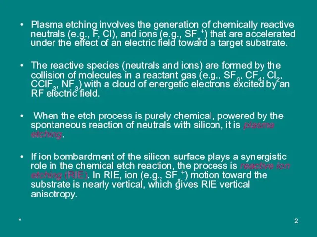
- 2. * Plasma etching involves the generation of chemically reactive neutrals (e.g., F, Cl), and ions (e.g.,
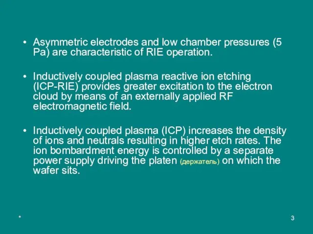
- 3. * Asymmetric electrodes and low chamber pressures (5 Pa) are characteristic of RIE operation. Inductively coupled
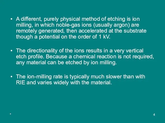
- 4. * A different, purely physical method of etching is ion milling, in which noble-gas ions (usually
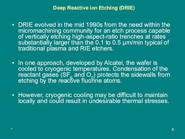
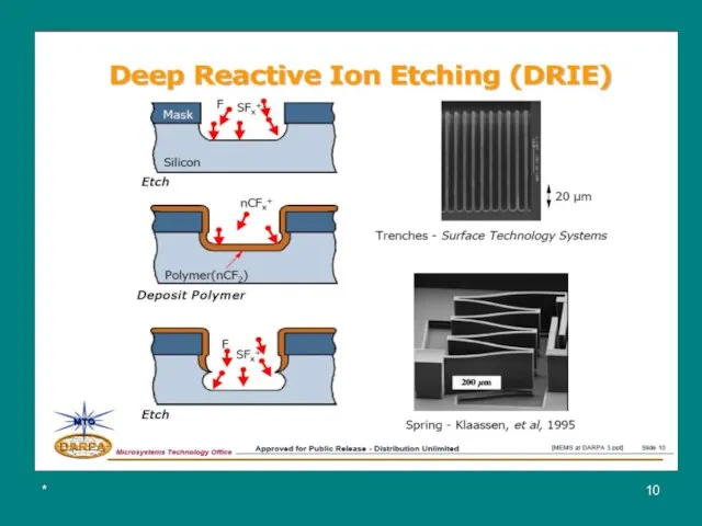
- 5. * Deep Reactive ion Etching (DRIE) DRIE evolved in the mid 1990s from the need within
- 6. * Another approach currently used by Alcatel, PlasmaTherm, and Surface Technology Systems (STS) follows a method
- 7. * The etch step has both vertical and isotropic character, resulting in a slight mask undercut
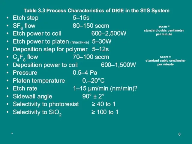
- 8. * Table 3.3 Process Characteristics of DRIE in the STS System Etch step 5–15s SF6 flow
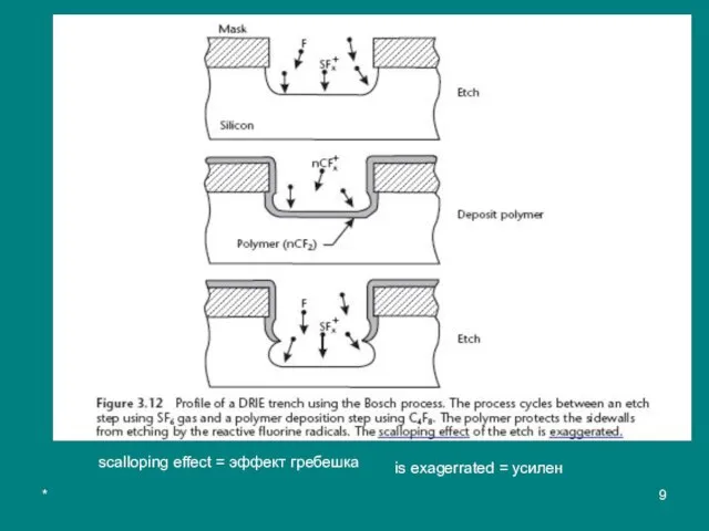
- 9. * scalloping effect = эффект гребешка is exagerrated = усилен
- 10. *
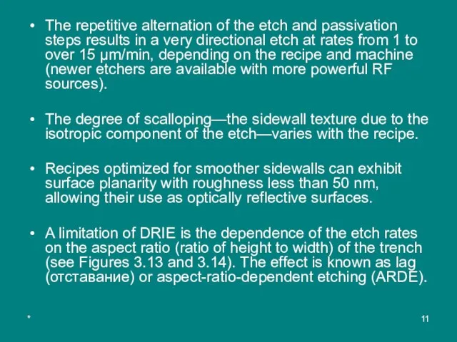
- 11. * The repetitive alternation of the etch and passivation steps results in a very directional etch
- 12. * The etch rate is limited by the flux of reactants (namely, F radicals) and drops
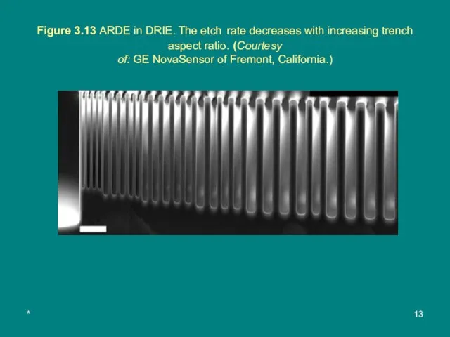
- 13. * Figure 3.13 ARDE in DRIE. The etch rate decreases with increasing trench aspect ratio. (Courtesy
- 14. *
- 15. * The high selectivity to silicon dioxide makes it possible to etch deep trenches and stop
- 16. *
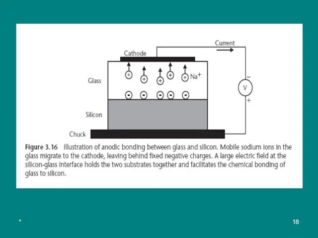
- 17. * Advanced Process Tools Anodic Bonding Anodic bonding, also known as field-assisted bonding or Mallory bonding,
- 18. *
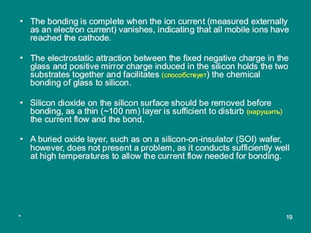
- 19. * The bonding is complete when the ion current (measured externally as an electron current) vanishes,
- 20. * The coefficient of thermal expansion of the glass substrate is preferably matched to that of
- 21. * Silicon Direct Bonding Silicon direct bonding, also known as silicon fusion bonding, is a process
- 22. * Silicon direct bonding can be performed between two bare single-crystal silicon surfaces or polished polysilicon.
- 23. * The direct bonding process starts with cleaning and hydration of the surfaces. The following is
- 24. * Finally, an RCA-2 clean (hot hydrochloric acid and hydrogen peroxide solution) is done to remove
- 25. * In some cases, features on the two bond surfaces must be aligned to each other
- 26. * A mechanical clamping fixture holds the aligned wafers in position, separated by thin spacers at
- 27. * Grinding (шлифовка), Polishing, and Chemical-Mechanical Polishing Some applications use a thin layer of silicon (5
- 28. * The thickness reduction is achieved using grinding and polishing. The wafer stack is mounted on
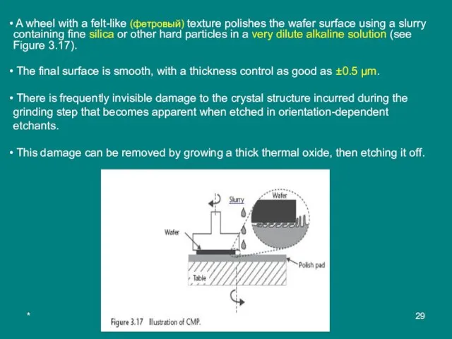
- 29. * A wheel with a felt-like (фетровый) texture polishes the wafer surface using a slurry containing
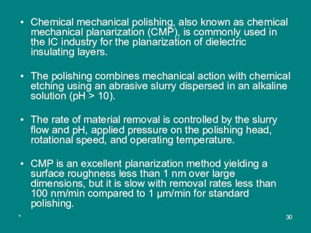
- 30. * Chemical mechanical polishing, also known as chemical mechanical planarization (CMP), is commonly used in the
- 31. * Водоро́дный показа́тель Водоро́дный показа́тель, pH (произносится «пэ аш», английское произношение англ. pH — pi:eɪtʃ —
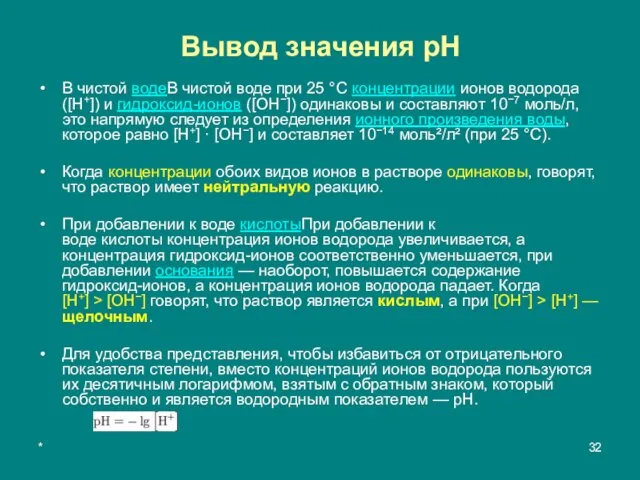
- 32. * Вывод значения pH В чистой водеВ чистой воде при 25 °C концентрации ионов водорода ([H+])
- 33. * Так как в кислых растворах [H+] > 10−7, то у кислых растворов pH 7. pH
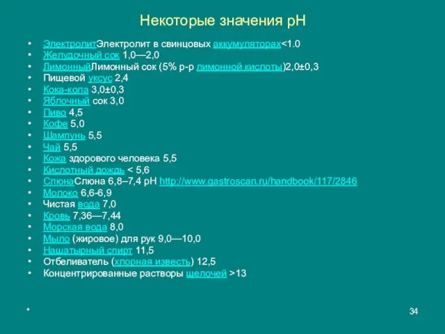
- 34. * Некоторые значения pH ЭлектролитЭлектролит в свинцовых аккумуляторах Желудочный сок 1,0—2,0 ЛимонныйЛимонный сок (5% р-р лимонной
- 35. * Sol-Gel Deposition Methods A sol-gel process is a chemical reaction between solid particles in colloidal
- 36. * A widespread application of sol-gel processing is in the coating of surfaces with optical absorption
- 37. * Electroceramic properties Being piezoelectricBeing piezoelectric, it develops a voltage (or potential difference) across two of
- 38. * Varieties of PZTs Сommonly studied chemical composition is PbСommonly studied chemical composition is PbZr0.52Ti0.48O3. The
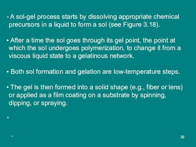
- 39. * A sol-gel process starts by dissolving appropriate chemical precursors in a liquid to form a
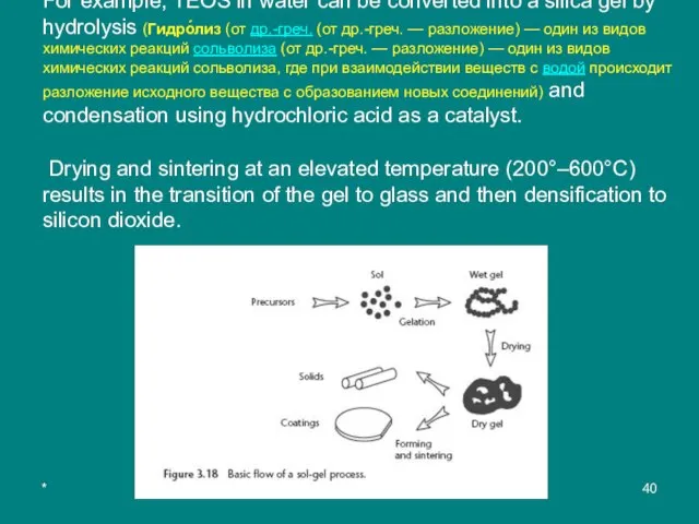
- 40. * For example, TEOS in water can be converted into a silica gel by hydrolysis (Гидро́лиз
- 41. * Silica gel is a granular is a granular, vitreous (стекловидный), porous, porous form of silicon
- 42. * Sodium silicate is the common name for a compound sodium metasilicate, Na2SiO3, also known as
- 44. Скачать презентацию
Слайд 3*
Asymmetric electrodes and low chamber pressures (5 Pa) are characteristic of RIE
*
Asymmetric electrodes and low chamber pressures (5 Pa) are characteristic of RIE
Слайд 4*
A different, purely physical method of etching is ion milling, in which
*
A different, purely physical method of etching is ion milling, in which
Слайд 5*
Deep Reactive ion Etching (DRIE)
DRIE evolved in the mid 1990s from
*
Deep Reactive ion Etching (DRIE)
DRIE evolved in the mid 1990s from
Слайд 6*
Another approach currently used by Alcatel, PlasmaTherm, and Surface Technology Systems (STS)
*
Another approach currently used by Alcatel, PlasmaTherm, and Surface Technology Systems (STS)
Слайд 7*
The etch step has both vertical and isotropic character, resulting in a
*
The etch step has both vertical and isotropic character, resulting in a
Слайд 8*
Table 3.3 Process Characteristics of DRIE in the STS System
Etch step
*
Table 3.3 Process Characteristics of DRIE in the STS System
Etch step
Слайд 9*
scalloping effect = эффект гребешка
is exagerrated = усилен
*
scalloping effect = эффект гребешка
is exagerrated = усилен
Слайд 11*
The repetitive alternation of the etch and passivation steps results in a
*
The repetitive alternation of the etch and passivation steps results in a
Слайд 12*
The etch rate is limited by the flux of reactants (namely, F
*
The etch rate is limited by the flux of reactants (namely, F
Слайд 13*
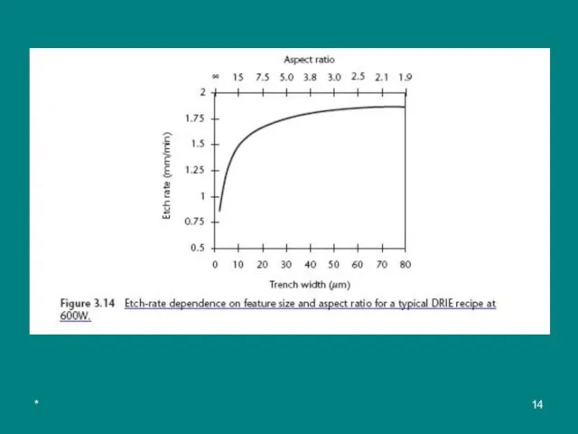
Figure 3.13 ARDE in DRIE. The etch rate decreases with increasing trench
*
Figure 3.13 ARDE in DRIE. The etch rate decreases with increasing trench
Слайд 15*
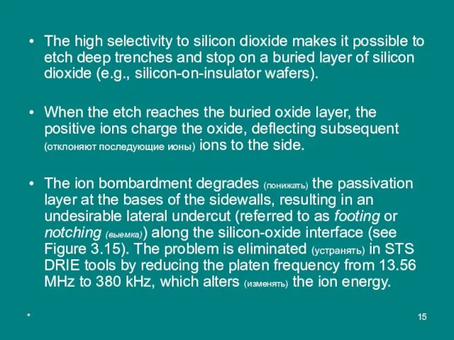
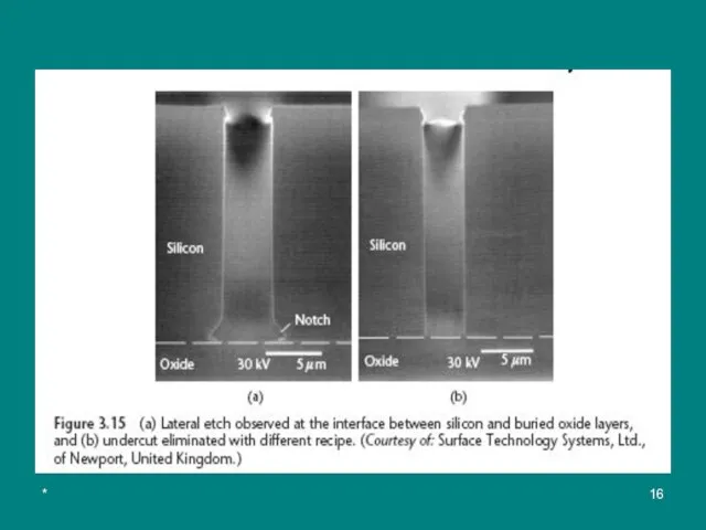
The high selectivity to silicon dioxide makes it possible to etch deep
*
The high selectivity to silicon dioxide makes it possible to etch deep
Слайд 17*
Advanced Process Tools
Anodic Bonding
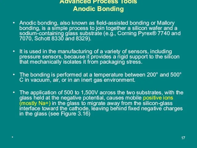
Anodic bonding, also known as field-assisted bonding or Mallory
*
Advanced Process Tools
Anodic Bonding
Anodic bonding, also known as field-assisted bonding or Mallory
Слайд 19*
The bonding is complete when the ion current (measured externally as an
*
The bonding is complete when the ion current (measured externally as an
Слайд 20*
The coefficient of thermal expansion of the glass substrate is preferably matched
*
The coefficient of thermal expansion of the glass substrate is preferably matched
Слайд 21*
Silicon Direct Bonding
Silicon direct bonding, also known as silicon fusion bonding, is
*
Silicon Direct Bonding
Silicon direct bonding, also known as silicon fusion bonding, is
Слайд 22*
Silicon direct bonding can be performed between two bare single-crystal silicon surfaces
*
Silicon direct bonding can be performed between two bare single-crystal silicon surfaces
Слайд 23*
The direct bonding process starts with cleaning and hydration of the surfaces.
The
*
The direct bonding process starts with cleaning and hydration of the surfaces.
The
Слайд 24*
Finally, an RCA-2 clean (hot hydrochloric acid and hydrogen peroxide solution) is
*
Finally, an RCA-2 clean (hot hydrochloric acid and hydrogen peroxide solution) is
Слайд 25*
In some cases, features on the two bond surfaces must be aligned
*
In some cases, features on the two bond surfaces must be aligned
Слайд 26*
A mechanical clamping fixture holds the aligned wafers in position, separated by
*
A mechanical clamping fixture holds the aligned wafers in position, separated by
Слайд 27*
Grinding (шлифовка), Polishing, and Chemical-Mechanical Polishing
Some applications use a thin layer of
*
Grinding (шлифовка), Polishing, and Chemical-Mechanical Polishing
Some applications use a thin layer of
Слайд 28*
The thickness reduction is achieved using grinding and polishing. The wafer stack
*
The thickness reduction is achieved using grinding and polishing. The wafer stack
Слайд 29*
A wheel with a felt-like (фетровый) texture polishes the wafer surface
*
A wheel with a felt-like (фетровый) texture polishes the wafer surface
Слайд 30*
Chemical mechanical polishing, also known as chemical mechanical planarization (CMP), is commonly
*
Chemical mechanical polishing, also known as chemical mechanical planarization (CMP), is commonly
Слайд 31*
Водоро́дный показа́тель
Водоро́дный показа́тель, pH (произносится «пэ аш», английское произношение англ. pH — pi:eɪtʃ — pi:eɪtʃ, «пи эйч») — мера активности — pi:eɪtʃ, «пи эйч») — мера активности (в очень разбавленных
*
Водоро́дный показа́тель
Водоро́дный показа́тель, pH (произносится «пэ аш», английское произношение англ. pH — pi:eɪtʃ — pi:eɪtʃ, «пи эйч») — мера активности — pi:eɪtʃ, «пи эйч») — мера активности (в очень разбавленных
Слайд 32*
Вывод значения pH
В чистой водеВ чистой воде при 25 °C концентрации ионов водорода ([H+]) и гидроксид-ионов ([OH−]) одинаковы и составляют
*
Вывод значения pH
В чистой водеВ чистой воде при 25 °C концентрации ионов водорода ([H+]) и гидроксид-ионов ([OH−]) одинаковы и составляют
Слайд 33*
Так как в кислых растворах [H+] > 10−7, то у кислых растворов
*
Так как в кислых растворах [H+] > 10−7, то у кислых растворов
![* Так как в кислых растворах [H+] > 10−7, то у кислых](/_ipx/f_webp&q_80&fit_contain&s_1440x1080/imagesDir/jpg/378459/slide-32.jpg)
Слайд 34*
Некоторые значения pH
ЭлектролитЭлектролит в свинцовых аккумуляторах<1.0
Желудочный сок 1,0—2,0
ЛимонныйЛимонный сок (5% р-р лимонной кислоты)2,0±0,3
Пищевой уксус 2,4
Кока-кола 3,0±0,3
Яблочный сок 3,0
Пиво
*
Некоторые значения pH
ЭлектролитЭлектролит в свинцовых аккумуляторах<1.0
Желудочный сок 1,0—2,0
ЛимонныйЛимонный сок (5% р-р лимонной кислоты)2,0±0,3
Пищевой уксус 2,4
Кока-кола 3,0±0,3
Яблочный сок 3,0
Пиво
Слайд 35*
Sol-Gel Deposition Methods
A sol-gel process is a chemical reaction between solid particles
*
Sol-Gel Deposition Methods
A sol-gel process is a chemical reaction between solid particles
Слайд 36*
A widespread application of sol-gel processing is in the coating of surfaces
*
A widespread application of sol-gel processing is in the coating of surfaces
Слайд 37*
Electroceramic properties
Being piezoelectricBeing piezoelectric, it develops a voltage (or potential difference) across two of its faces
*
Electroceramic properties
Being piezoelectricBeing piezoelectric, it develops a voltage (or potential difference) across two of its faces
Слайд 38*
Varieties of PZTs
Сommonly studied chemical composition is PbСommonly studied chemical composition is PbZr0.52Ti0.48O3. The
*
Varieties of PZTs
Сommonly studied chemical composition is PbСommonly studied chemical composition is PbZr0.52Ti0.48O3. The
Слайд 39*
A sol-gel process starts by dissolving appropriate chemical precursors in a
*
A sol-gel process starts by dissolving appropriate chemical precursors in a
Слайд 40*
For example, TEOS in water can be converted into a silica gel
*
For example, TEOS in water can be converted into a silica gel
Слайд 41*
Silica gel is a granular is a granular, vitreous (стекловидный), porous, porous form of silicon dioxide, porous form of silicon dioxide made synthetically from sodium silicate.
Silica
*
Silica gel is a granular is a granular, vitreous (стекловидный), porous, porous form of silicon dioxide, porous form of silicon dioxide made synthetically from sodium silicate.
Silica
Слайд 42*
Sodium silicate is the common name for a compound sodium metasilicate, Na2SiO3, also
*
Sodium silicate is the common name for a compound sodium metasilicate, Na2SiO3, also
 Будни и праздники начальной школы
 Масленица
 Тренинг для собственников и топ - менеджеров компаний
 Инновационный менеджмент в образовании
 МОУ «Средняя общеобразовательная школа №7»г. Сосновый Бор Ленинградской областиПроектно– исследовательская работапо биологи
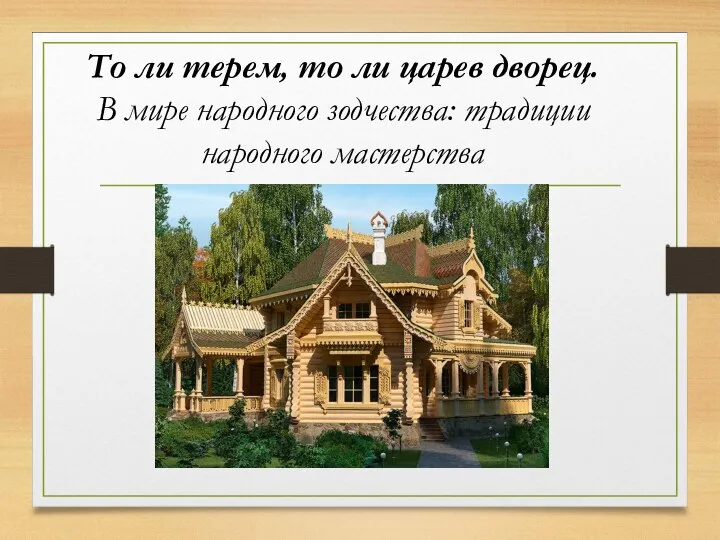 В мире народного зодчества: традиции народного мастерства
 Служба ценового мониторингаОГУ «Самара-АРИС»
 ПЕРИОДЫ ДЕТСКОГО ВОЗРАСТА. ЗНАЧЕНИЕ ГЕНЕТИЧЕСКИХ И НАСЛЕДСТВЕННЫХ факторов
  Поведение во время грозы
 Государственная символика Российской Федерации. География и право вокруг нас
 Психологические аспекты неуспеваемости И пути ее предупреждения
 Субъекты и объекты гражданского права
 Презентация на тему Семья в современном обществе. Законодательство о семье
 Книги о войне
 Семейное право как отрасль права
 Домашние метеостанции
 Пожары на объектах добычи и хранения жидкого и газообразного топлива
  Задание на позицию менеджера проектов
 Презентация на тему Международно-правовое регулирование торговли услугами
 Риск-ориентированный подход в системе контроля эффективности деятельности образовательных организаций
 Природные явления. Землетрясения и вулканы
 Требования к результатам освоения основных образовательных программ
 Отдельные заметки к решениям казусов
 Индейцы
 Дроздов Савченко
 презентация
 Введение в отрасль уголовного процесса
 Оценка инвестиционного потенциала Украины: отраслевой аспект