- Etching

Содержание
- 2. * Isotropic Wet Etching The most common group of silicon isotropic wet etchants is HNA, also
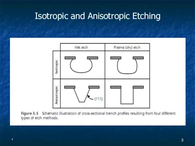
- 3. * Isotropic and Anisotropic Etching
- 4. * Anisotropic wet etchants Anisotropic wet etchants are also known as orientation-dependent etchants (ODEs) because their
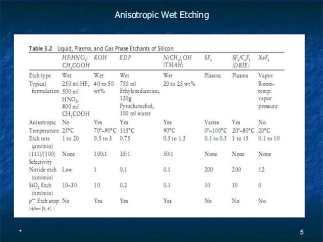
- 5. * Anisotropic Wet Etching
- 6. * KOH is by far the most common ODE Etch rates are typically given in the
- 7. * Anisotropic Etching of Crystalline Silicon in Alkaline Solutions I. Orientation Dependence and Behavior of Passivation
- 8. * In an oxidation step, four hydroxide ions react with one surface silicon atom, leading to
- 9. * Etch rate of Si in KOH Depends on Crystallographic Plane
- 10. * Etch rate of Si in KOH Depends on Temperature
- 11. * Etch Rate of Oxide in KOH
- 12. * The etch rate of KOH and other alkaline etchants also slows greatly for heavily doped
- 13. * Anisotropic Etching of Crystalline Silicon in Alkaline Solutions II. Influence of Dopants J. Electrochem. Soc.,
- 14. * On the basis of these results, a model is proposed attributing the etch stop phenomenon
- 15. *
- 16. * Anisotropic Etch Stop Layers - 1 Controlling the absolute depth of an etch is often
- 17. *
- 18. * Oblique [эблик] = скошенный
- 19. * Alkali hydroxides are extremely corrosive; aluminum bond pads inadvertently exposed to KOH are quickly damaged.
- 20. * In the category of ammonium hydroxides, tetramethyl ammonium hydroxide (TMAH, N(CH3)4OH) exhibits similar properties to
- 21. * Both silicon dioxide and silicon nitride remain virtually unetched in TMAH and hence can be
- 22. * EDP is another wet etchant with selectivity to {111} planes and to heavily p-doped silicon.
- 23. * Etching using anisotropic aqueous solutions results in three-dimensional faceted structures formed by intersecting {111} planes
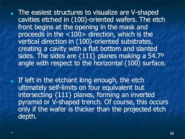
- 24. * The easiest structures to visualize are V-shaped cavities etched in (100)-oriented wafers. The etch front
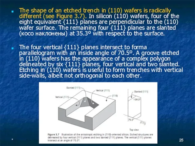
- 25. * The shape of an etched trench in (110) wafers is radically different (see Figure 3.7).
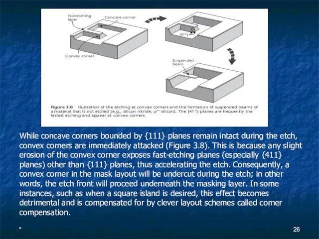
- 26. * While concave corners bounded by {111} planes remain intact during the etch, convex corners are
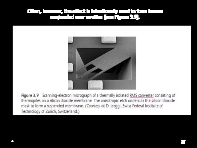
- 27. * Often, however, the effect is intentionally used to form beams suspended over cavities (see Figure
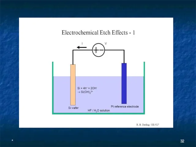
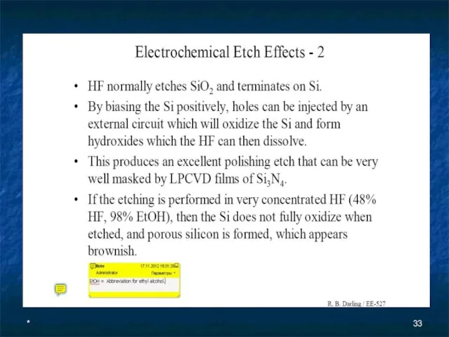
- 28. * Electrochemical Etching (ECE) The relatively large etch rates of anisotropic wet etchants (>0.5 µm/min) make
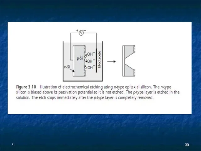
- 29. * An n-type epitaxial layer grown on a p-type wafer forms a p-n junction diode that
- 30. *
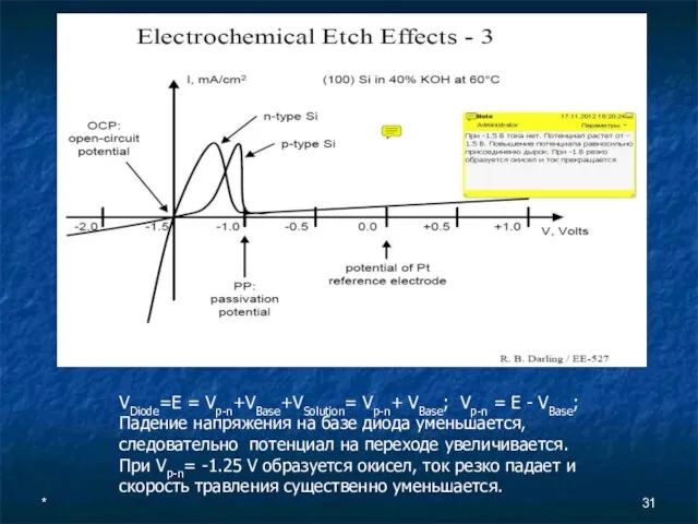
- 31. * VDiode=E = Vp-n+VBase+VSolution= Vp-n+ VBase; Vp-n = E - VBase; Падение напряжения на базе диода
- 32. *
- 33. *
- 35. Скачать презентацию
Слайд 3*
Isotropic and Anisotropic Etching
*
Isotropic and Anisotropic Etching
Слайд 4*
Anisotropic wet etchants
Anisotropic wet etchants are also known as orientation-dependent etchants (ODEs)
*
Anisotropic wet etchants
Anisotropic wet etchants are also known as orientation-dependent etchants (ODEs)
Слайд 5*
Anisotropic Wet Etching
*
Anisotropic Wet Etching
Слайд 6*
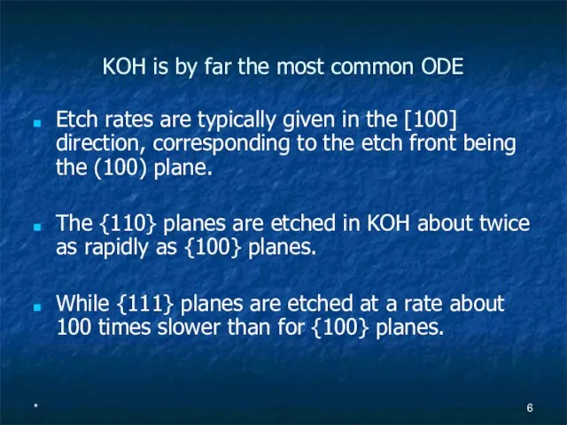
KOH is by far the most common ODE
Etch rates are typically given
*
KOH is by far the most common ODE
Etch rates are typically given
Слайд 7*
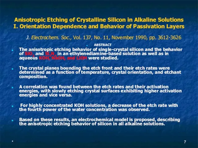
Anisotropic Etching of Crystalline Silicon in Alkaline Solutions
I. Orientation Dependence and Behavior
*
Anisotropic Etching of Crystalline Silicon in Alkaline Solutions I. Orientation Dependence and Behavior
Слайд 8*
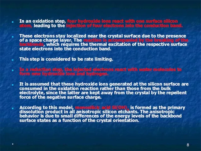
In an oxidation step, four hydroxide ions react with one surface silicon
*
In an oxidation step, four hydroxide ions react with one surface silicon
Слайд 9*
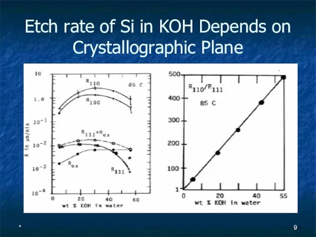
Etch rate of Si in KOH Depends on
Crystallographic Plane
*
Etch rate of Si in KOH Depends on
Crystallographic Plane
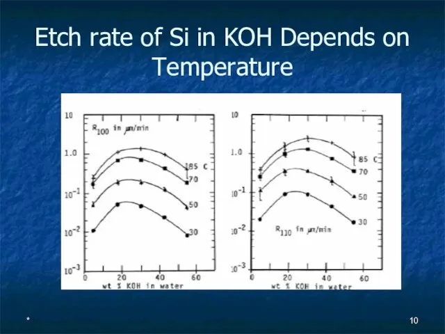
Слайд 10*
Etch rate of Si in KOH Depends on
Temperature
*
Etch rate of Si in KOH Depends on
Temperature
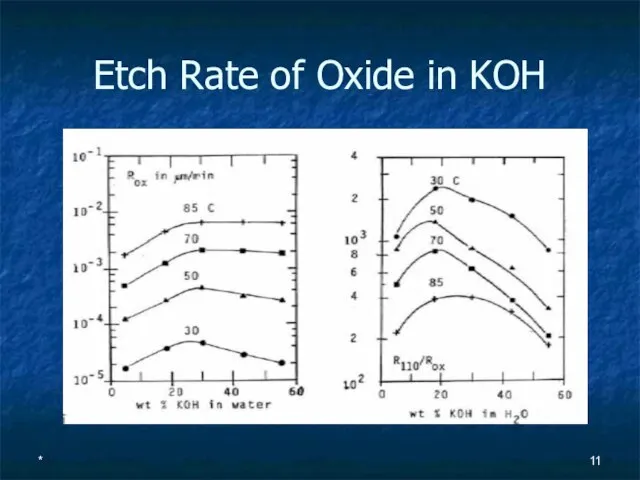
Слайд 11*
Etch Rate of Oxide in KOH
*
Etch Rate of Oxide in KOH
Слайд 12*
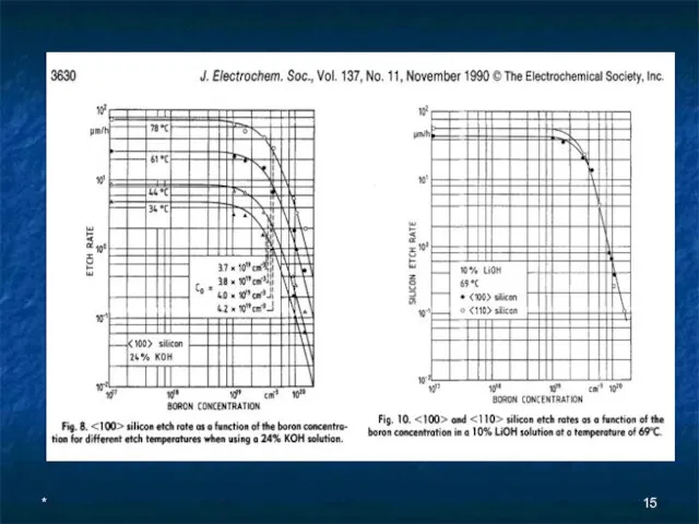
The etch rate of KOH and other alkaline etchants also slows greatly
*
The etch rate of KOH and other alkaline etchants also slows greatly
Слайд 13*
Anisotropic Etching of Crystalline Silicon in Alkaline Solutions
II. Influence of Dopants
*
Anisotropic Etching of Crystalline Silicon in Alkaline Solutions II. Influence of Dopants
Слайд 14*
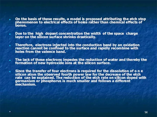
On the basis of these results, a model is proposed attributing the
*
On the basis of these results, a model is proposed attributing the
Слайд 16*
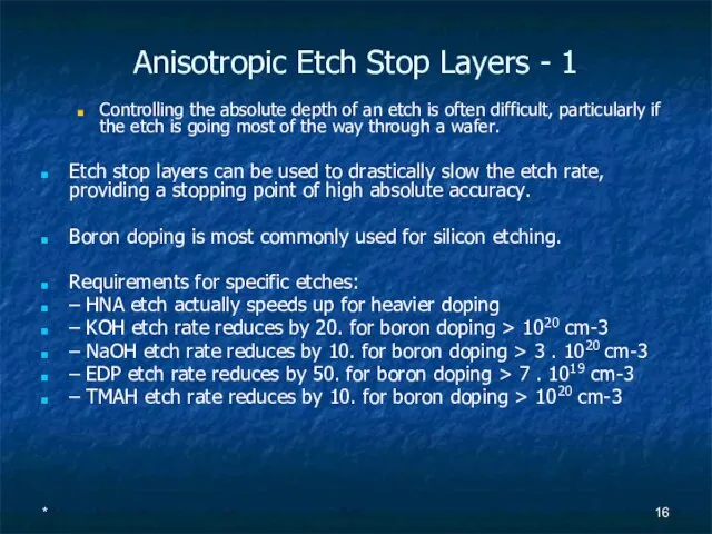
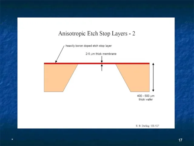
Anisotropic Etch Stop Layers - 1
Controlling the absolute depth of an etch
*
Anisotropic Etch Stop Layers - 1
Controlling the absolute depth of an etch
Слайд 18*
Oblique [эблик] = скошенный
*
Oblique [эблик] = скошенный
![* Oblique [эблик] = скошенный](/_ipx/f_webp&q_80&fit_contain&s_1440x1080/imagesDir/jpg/378458/slide-17.jpg)
Слайд 19*
Alkali hydroxides are extremely corrosive; aluminum bond pads inadvertently exposed to KOH
*
Alkali hydroxides are extremely corrosive; aluminum bond pads inadvertently exposed to KOH

Слайд 20*
In the category of ammonium hydroxides, tetramethyl ammonium hydroxide (TMAH, N(CH3)4OH) exhibits
*
In the category of ammonium hydroxides, tetramethyl ammonium hydroxide (TMAH, N(CH3)4OH) exhibits
Слайд 21*
Both silicon dioxide and silicon nitride remain virtually unetched in TMAH and
*
Both silicon dioxide and silicon nitride remain virtually unetched in TMAH and
Слайд 22*
EDP is another wet etchant with selectivity to {111} planes and to
*
EDP is another wet etchant with selectivity to {111} planes and to
Слайд 23*
Etching using anisotropic aqueous solutions results in three-dimensional faceted structures formed by
*
Etching using anisotropic aqueous solutions results in three-dimensional faceted structures formed by
Слайд 24*
The easiest structures to visualize are V-shaped cavities etched in (100)-oriented wafers.
*
The easiest structures to visualize are V-shaped cavities etched in (100)-oriented wafers.
Слайд 25*
The shape of an etched trench in (110) wafers is radically different
*
The shape of an etched trench in (110) wafers is radically different
Слайд 26*
While concave corners bounded by {111} planes remain intact during the etch,
*
While concave corners bounded by {111} planes remain intact during the etch,
Слайд 27*
Often, however, the effect is intentionally used to form beams suspended over
*
Often, however, the effect is intentionally used to form beams suspended over
Слайд 28*
Electrochemical Etching (ECE)
The relatively large etch rates of anisotropic wet etchants (>0.5
*
Electrochemical Etching (ECE)
The relatively large etch rates of anisotropic wet etchants (>0.5
Слайд 29*
An n-type epitaxial layer grown on a p-type wafer forms a
*
An n-type epitaxial layer grown on a p-type wafer forms a
Слайд 31*
VDiode=E = Vp-n+VBase+VSolution= Vp-n+ VBase; Vp-n = E - VBase; Падение напряжения
*
VDiode=E = Vp-n+VBase+VSolution= Vp-n+ VBase; Vp-n = E - VBase; Падение напряжения
 Будни и праздники начальной школы
 Масленица
 Тренинг для собственников и топ - менеджеров компаний
 Инновационный менеджмент в образовании
 МОУ «Средняя общеобразовательная школа №7»г. Сосновый Бор Ленинградской областиПроектно– исследовательская работапо биологи
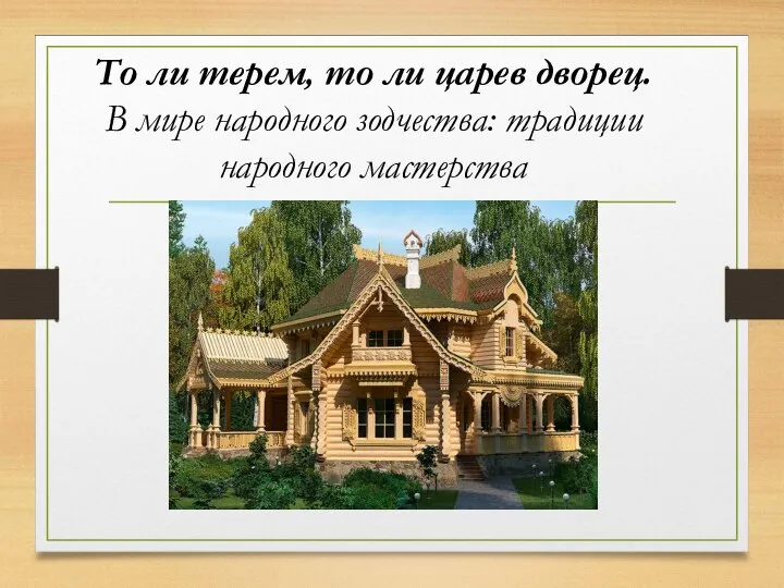 В мире народного зодчества: традиции народного мастерства
 Служба ценового мониторингаОГУ «Самара-АРИС»
 ПЕРИОДЫ ДЕТСКОГО ВОЗРАСТА. ЗНАЧЕНИЕ ГЕНЕТИЧЕСКИХ И НАСЛЕДСТВЕННЫХ факторов
  Поведение во время грозы
 Государственная символика Российской Федерации. География и право вокруг нас
 Психологические аспекты неуспеваемости И пути ее предупреждения
 Субъекты и объекты гражданского права
 Презентация на тему Семья в современном обществе. Законодательство о семье
 Книги о войне
 Семейное право как отрасль права
 Домашние метеостанции
 Пожары на объектах добычи и хранения жидкого и газообразного топлива
  Задание на позицию менеджера проектов
 Презентация на тему Международно-правовое регулирование торговли услугами
 Риск-ориентированный подход в системе контроля эффективности деятельности образовательных организаций
 Природные явления. Землетрясения и вулканы
 Требования к результатам освоения основных образовательных программ
 Отдельные заметки к решениям казусов
 Индейцы
 Дроздов Савченко
 презентация
 Введение в отрасль уголовного процесса
 Оценка инвестиционного потенциала Украины: отраслевой аспект