- Porous Silicon

Содержание
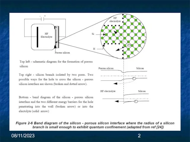
- 2. 08/11/2023
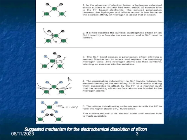
- 3. 08/11/2023 Suggested mechanism for the electrochemical dissolution of silicon
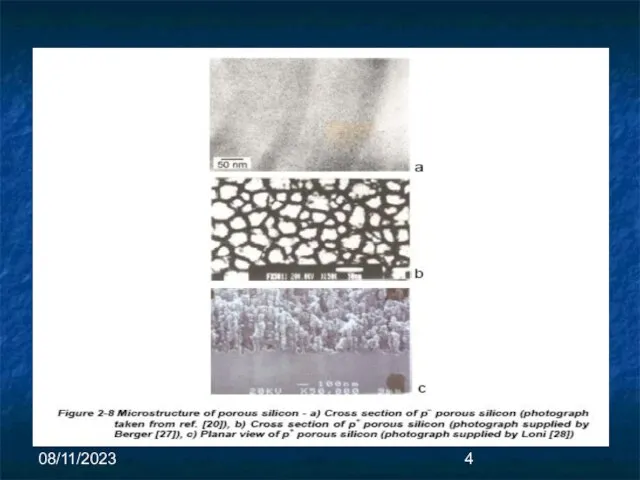
- 4. 08/11/2023
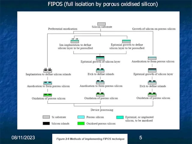
- 5. 08/11/2023 FIPOS (full isolation by porous oxidised silicon)
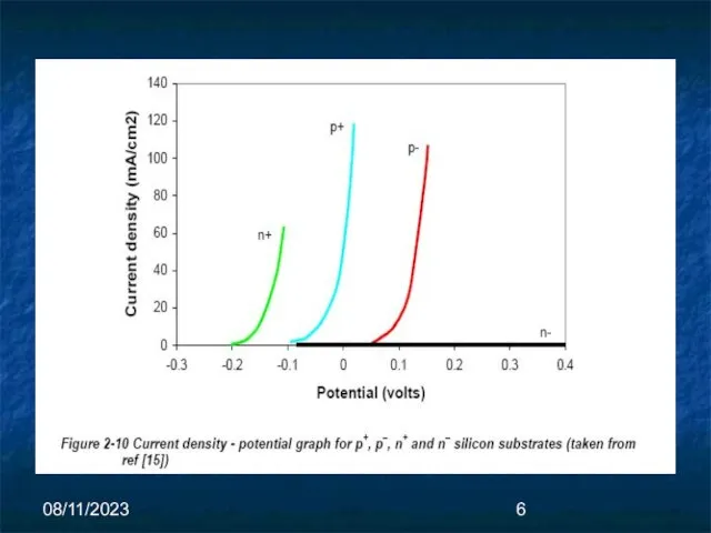
- 6. 08/11/2023
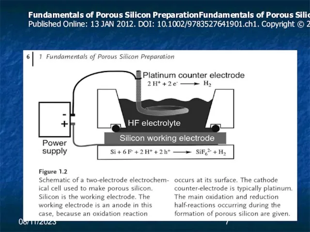
- 7. 08/11/2023 Fundamentals of Porous Silicon PreparationFundamentals of Porous Silicon Preparation. Prof. Dr. Michael J. Sailor. Published
- 8. 08/11/2023 The techniques employed for dielectric isolation using porous silicon can also be used for micromachining
- 9. 08/11/2023 For high current densities, the density of holes is high and the etched surface is
- 10. 08/11/2023 The large surface-to-volume ratios make porous Si attractive for gaseous and liquid applications, including filter
- 11. 08/11/2023 A third application uses porous Si as a sacrificial layer for polysilicon and single crystalline
- 12. 08/11/2023 Silicon Dioxide Silicon dioxide (SiO2) is one of the most widely used materials in the
- 13. 08/11/2023 The most common processes used to produce SiO2 films for polysilicon surface micromachining are thermal
- 14. 08/11/2023 SiO2 films can be deposited on a wide variety of substrate materials by LPCVD. LPCVD
- 15. 08/11/2023 Phosphosilicate glass (PSG) can be formed using nearly the same deposition process as LTO by
- 16. 08/11/2023 PSG and LTO films are deposited in hot-wall, low pressure, fused silica furnaces in systems
- 17. 08/11/2023 The low deposition temperatures result in LTO and PSG films that are slightly less dense
- 18. 08/11/2023 Thermal SiO2 and LTO are electrical insulators used in numerous MEMS applications. The dielectric constants
- 19. 08/11/2023 For LTO the as-deposited residual stress is tensile, with a magnitude of about 100 MPa
- 20. 08/11/2023 Plasma-enhanced chemical vapor deposition (PECVD) is another common method to produce oxides of silicon. Using
- 21. 08/11/2023 Quartz is the crystalline form of SiO2 and has interesting properties for MEMS. Quartz is
- 22. 08/11/2023 Another SiO2-related material that has recently found uses in MEMS is spin-on-glass (SOG). SOG is
- 23. 08/11/2023 The thick SOG films were patterned into molds and filled with 10 micron-thick LPCVD polysilicon
- 24. 08/11/2023 In the second example, Liu et al. fabricated high-aspect ratio channel plate microstructures from SOG.
- 25. 08/11/2023 Thick (5–100 µm) spin-on glass (SOG) has the ability to uniformly coat surfaces and smooth
- 26. 08/11/2023 Spin-on glass is commercially available in different forms, commonly siloxane- or silicate-based. The latter type
- 27. 08/11/2023 Spin on glass (SOG) is a mixture of SiO2 and dopants (either boron or phosphorous)
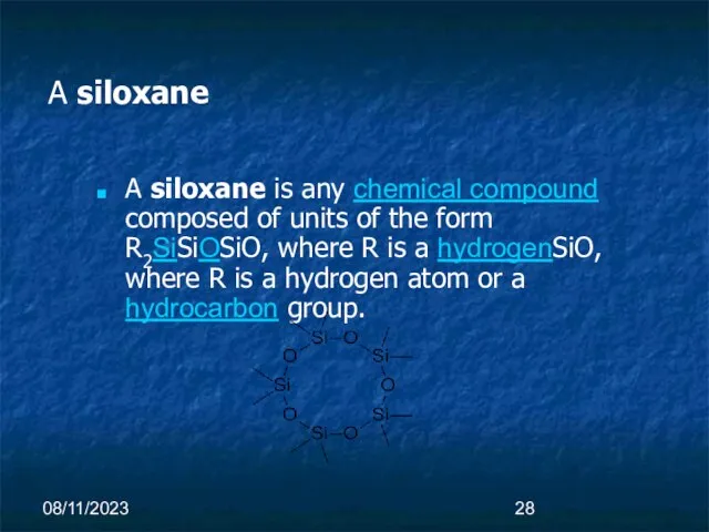
- 28. 08/11/2023 A siloxane A siloxane is any chemical compound composed of units of the form R2SiSiOSiO,
- 29. 08/11/2023 An examples are: [SiO(CH3)2]n (polydimethylsiloxane) and [SiO(C6H5)2]n (polydiphenylsiloxane).
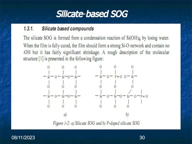
- 30. 08/11/2023 Silicate-based SOG
- 31. 08/11/2023 Silicon Nitride Silicon nitride (Si3N4) is widely used in MEMS for electrical isolation, surface passivation,
- 32. 08/11/2023 PECVD silicon nitride is generally nonstoichiometric (sometimes denoted as SixNy : H) and may contain
- 33. 08/11/2023 Unlike its PECVD counterpart, LPCVD Si3N4 is extremely resistant to chemical attack, making it the
- 34. 08/11/2023 Typical deposition temperatures and pressures range between 700 ◦C to 900 ◦C and 200 mtorr
- 35. 08/11/2023 The residual stress in stoichiometric Si3N4 is large and tensile, with a magnitude of about
- 36. 08/11/2023 Стехиометрия (от др.-греч. (от др.-греч. στοιχεῖον «элемент» + μετρέω «измерять») — раздел химии (от др.-греч.
- 37. 08/11/2023 Рассмотрим реакцию термитной смеси: Fe2O3 + 2Al → Al2O3 + 2Fe. Сколько граммов алюминия нам
- 38. 08/11/2023 To enable the use of Si3N4 films for applications that require micron thick, durable (прочные),
- 39. 08/11/2023 Nearly stress-free films can be deposited using a NH3 to SiH2Cl2 ratio of 1 :
- 40. 08/11/2023 Germanium-Based Materials Like Si, Ge has a long history as a semiconductor device material, dating
- 41. 08/11/2023 Polycrystalline Ge Thin polycrystalline Ge (poly-Ge) films can be deposited by LPCVD at temperatures as
- 42. 08/11/2023 Poly-Ge is essentially impervious (невосприимчивый) to KOH, TMAH, and BOE, enabling the fabrication of Ge
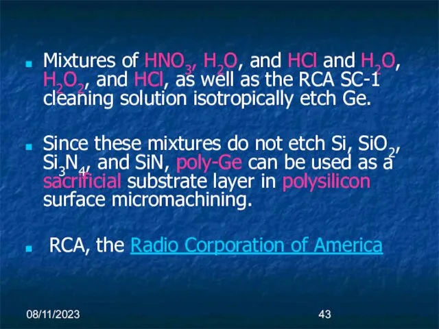
- 43. 08/11/2023 Mixtures of HNO3, H2O, and HCl and H2O, H2O2, and HCl, as well as the
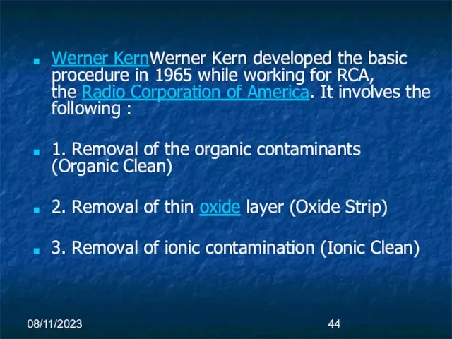
- 44. 08/11/2023 Werner KernWerner Kern developed the basic procedure in 1965 while working for RCA, the Radio
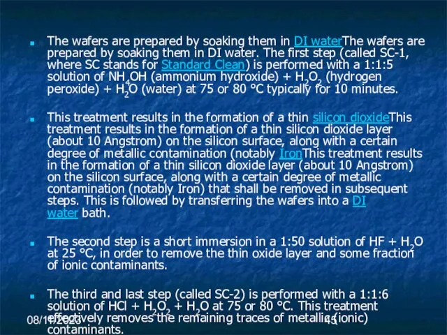
- 45. 08/11/2023 The wafers are prepared by soaking them in DI waterThe wafers are prepared by soaking
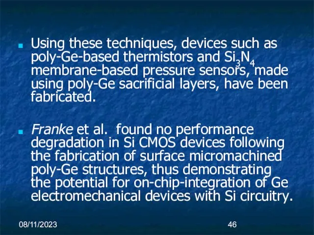
- 46. 08/11/2023 Using these techniques, devices such as poly-Ge-based thermistors and Si3N4 membrane-based pressure sensors, made using
- 47. 08/11/2023 Polycrystalline SiGe Like poly-Ge, polycrystalline SiGe (poly-SiGe) is a material that can be deposited at
- 48. 08/11/2023 In general, the deposition temperature is related to the concentration of Ge in the films,
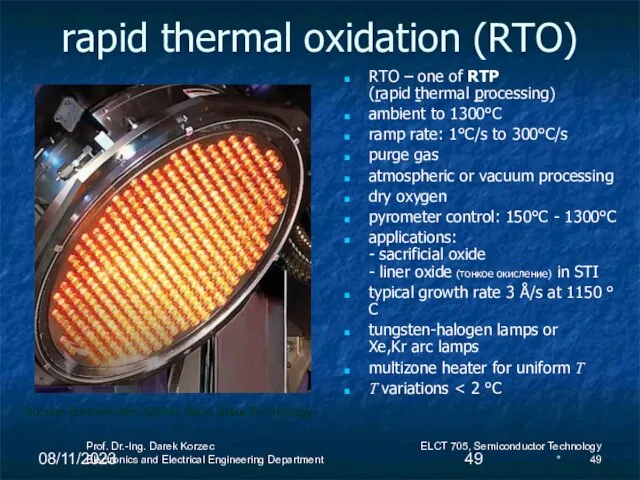
- 49. 08/11/2023 Prof. Dr.-Ing. Darek Korzec Electronics and Electrical Engineering Department ELCT 705, Semiconductor Technology * rapid
- 50. 08/11/2023 Like polysilicon, poly-SiGe can be doped with boron and phosphorus to modify its conductivity. In
- 51. 08/11/2023 Unlike poly-Ge, poly-SiGe can be deposited on a number of sacrificial substrates, including SiO2, PSG,
- 52. 08/11/2023 For instance, etching of poly-SiGe by H2O2 becomes significant for Ge concentrations over 70%. Sedky
- 53. 08/11/2023 The poly-SiGe, poly-Ge material system is particularly attractive for surface micromachining since H2O2 can be
- 54. 08/11/2023 Due to the conformal nature of LPCVD processing, poly-SiGe structural elements, such as gimbal-based microactuator
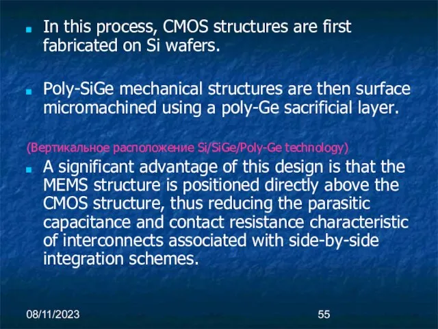
- 55. 08/11/2023 In this process, CMOS structures are first fabricated on Si wafers. Poly-SiGe mechanical structures are
- 56. 08/11/2023 Use of H2O2 as the sacrificial etchant means that no special protective layers are required
- 57. 08/11/2023 Metals Metallic thin films are used in many different capacities ranging from etch masks used
- 58. 08/11/2023
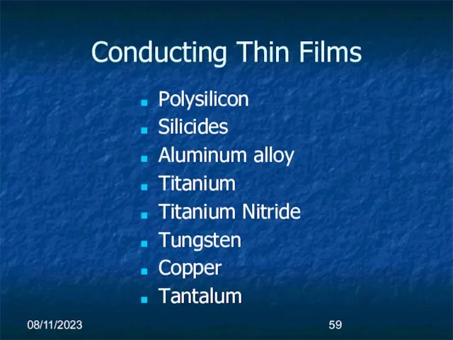
- 59. 08/11/2023 Polysilicon Silicides Aluminum alloy Titanium Titanium Nitride Tungsten Copper Tantalum Conducting Thin Films
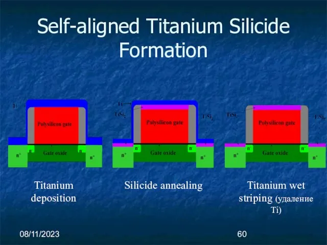
- 60. 08/11/2023 Self-aligned Titanium Silicide Formation
- 61. 08/11/2023 CMOS: Standard Metallization P-wafer N-Well P-Well STI n+ n+ USG p+ p+ Metal 1, Al•Cu
- 62. 08/11/2023 Fluorosilicate glass (FSG) is a low-k dielectric (FSG) is a low-k dielectric used in between
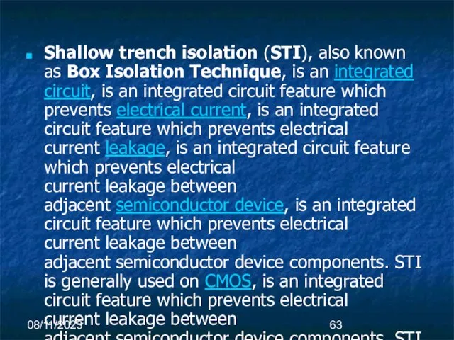
- 63. 08/11/2023 Shallow trench isolation (STI), also known as Box Isolation Technique, is an integrated circuit, is
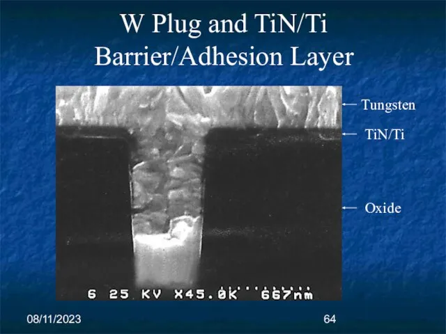
- 64. 08/11/2023 W Plug and TiN/Ti Barrier/Adhesion Layer
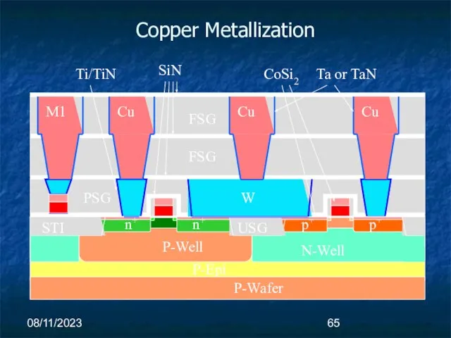
- 65. 08/11/2023 Copper Metallization
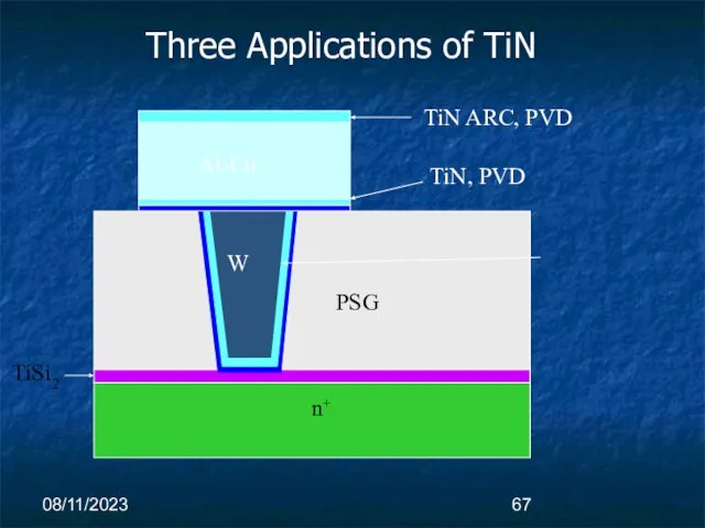
- 66. 08/11/2023 Applications of Titanium Ti PSG TiSi 2 n + Ti W Al-Cu
- 67. 08/11/2023 PSG TiSi2 n + TiN, PVD W Al-Cu TiN ARC, PVD Three Applications of TiN
- 68. 08/11/2023 Aluminum (Al) and gold (Au) are among the most widely employed metals in microfabricated electronic
- 69. 08/11/2023 One such example is the use of Au micromechanical switches for RF MEMS. For conventional
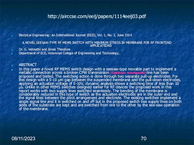
- 70. 08/11/2023 http://airccse.com/eeij/papers/1114eeij03.pdf Electrical Engineering: An International Journal (EEIJ), Vol. 1, No. 1, June 2014 A NOVEL
- 71. 08/11/2023 Unfortunately, these devices suffer (страдают) from insertion losses and poor electrical solation. In an effort
- 72. 08/11/2023 The trilayer cantilever structure was chosen to minimize the deleterious effects of thermal and process-related
- 73. 08/11/2023 The processing steps proved to be completely compatible with GaAs substrates. The released cantilevers demonstrated
- 74. 08/11/2023 In a second example from RF MEMS, Chang et al. reported the fabrication of an
- 75. 08/11/2023 Each switch is comprised of a series of linked bimorph cantilevers designed in such a
- 76. 08/11/2023 The released switches were relatively slow, at 10ms, but an actuation voltage of only 26V
- 77. 08/11/2023 The reversible phase change allows the shape-memory effect to be used as an actuation mechanism,
- 78. 08/11/2023 Titanium-nickel (TiNi) is among the most popular of the shape-memory alloys, owing to its high
- 79. 08/11/2023 In this study, TiNi films were deposited by co-sputtering elemental Ti and Ni targets, and
- 81. Скачать презентацию
Слайд 308/11/2023
Suggested mechanism for the electrochemical dissolution of silicon
08/11/2023
Suggested mechanism for the electrochemical dissolution of silicon
Слайд 408/11/2023
08/11/2023
Слайд 508/11/2023
FIPOS (full isolation by porous oxidised silicon)
08/11/2023
FIPOS (full isolation by porous oxidised silicon)
Слайд 608/11/2023
08/11/2023
Слайд 708/11/2023
Fundamentals of Porous Silicon PreparationFundamentals of Porous Silicon Preparation. Prof. Dr. Michael
08/11/2023
Fundamentals of Porous Silicon PreparationFundamentals of Porous Silicon Preparation. Prof. Dr. Michael
Слайд 808/11/2023
The techniques employed for dielectric isolation using porous silicon can also be
08/11/2023
The techniques employed for dielectric isolation using porous silicon can also be
Слайд 908/11/2023
For high current densities, the density of holes is high and the
08/11/2023
For high current densities, the density of holes is high and the
Слайд 1008/11/2023
The large surface-to-volume ratios make porous Si attractive for gaseous and liquid
08/11/2023
The large surface-to-volume ratios make porous Si attractive for gaseous and liquid
Слайд 1108/11/2023
A third application uses porous Si as a sacrificial layer for polysilicon
08/11/2023
A third application uses porous Si as a sacrificial layer for polysilicon
Слайд 1208/11/2023
Silicon Dioxide
Silicon dioxide (SiO2) is one of the most widely used materials
08/11/2023
Silicon Dioxide
Silicon dioxide (SiO2) is one of the most widely used materials
Слайд 1308/11/2023
The most common processes used to produce SiO2 films for polysilicon surface
08/11/2023
The most common processes used to produce SiO2 films for polysilicon surface
Слайд 1408/11/2023
SiO2 films can be deposited on a wide variety of substrate materials
08/11/2023
SiO2 films can be deposited on a wide variety of substrate materials
Слайд 1508/11/2023
Phosphosilicate glass (PSG) can be formed using nearly the same deposition process
08/11/2023
Phosphosilicate glass (PSG) can be formed using nearly the same deposition process
Слайд 1608/11/2023
PSG and LTO films are deposited in hot-wall, low pressure, fused silica
08/11/2023
PSG and LTO films are deposited in hot-wall, low pressure, fused silica
Слайд 1708/11/2023
The low deposition temperatures result in LTO and PSG films that are
08/11/2023
The low deposition temperatures result in LTO and PSG films that are
Слайд 1808/11/2023
Thermal SiO2 and LTO are electrical insulators used in numerous MEMS applications.
The
08/11/2023
Thermal SiO2 and LTO are electrical insulators used in numerous MEMS applications.
The
Слайд 1908/11/2023
For LTO the as-deposited residual stress is tensile, with a magnitude of
08/11/2023
For LTO the as-deposited residual stress is tensile, with a magnitude of
Слайд 2008/11/2023
Plasma-enhanced chemical vapor deposition (PECVD) is another common method to produce oxides
08/11/2023
Plasma-enhanced chemical vapor deposition (PECVD) is another common method to produce oxides
Слайд 2108/11/2023
Quartz is the crystalline form of SiO2 and has interesting properties for
08/11/2023
Quartz is the crystalline form of SiO2 and has interesting properties for
Слайд 2208/11/2023
Another SiO2-related material that has recently found uses in MEMS is spin-on-glass
08/11/2023
Another SiO2-related material that has recently found uses in MEMS is spin-on-glass
Слайд 2308/11/2023
The thick SOG films were patterned into molds and filled with 10
08/11/2023
The thick SOG films were patterned into molds and filled with 10
Слайд 2408/11/2023
In the second example, Liu et al. fabricated high-aspect ratio channel plate
08/11/2023
In the second example, Liu et al. fabricated high-aspect ratio channel plate
Слайд 2508/11/2023
Thick (5–100 µm) spin-on glass (SOG) has the ability to uniformly coat
08/11/2023
Thick (5–100 µm) spin-on glass (SOG) has the ability to uniformly coat
Слайд 2608/11/2023
Spin-on glass is commercially available in different forms, commonly siloxane- or silicate-based.
08/11/2023
Spin-on glass is commercially available in different forms, commonly siloxane- or silicate-based.
Слайд 2708/11/2023
Spin on glass (SOG) is a mixture of SiO2 and dopants (either
08/11/2023
Spin on glass (SOG) is a mixture of SiO2 and dopants (either
Слайд 2808/11/2023
A siloxane
A siloxane is any chemical compound composed of units of the
08/11/2023
A siloxane
A siloxane is any chemical compound composed of units of the
Слайд 2908/11/2023
An examples are: [SiO(CH3)2]n (polydimethylsiloxane)
and [SiO(C6H5)2]n (polydiphenylsiloxane).
08/11/2023
An examples are: [SiO(CH3)2]n (polydimethylsiloxane)
and [SiO(C6H5)2]n (polydiphenylsiloxane).
![08/11/2023 An examples are: [SiO(CH3)2]n (polydimethylsiloxane) and [SiO(C6H5)2]n (polydiphenylsiloxane).](/_ipx/f_webp&q_80&fit_contain&s_1440x1080/imagesDir/jpg/373792/slide-28.jpg)
Слайд 3008/11/2023
Silicate-based SOG
08/11/2023
Silicate-based SOG
Слайд 3108/11/2023
Silicon Nitride
Silicon nitride (Si3N4) is widely used in MEMS for electrical isolation,
08/11/2023
Silicon Nitride
Silicon nitride (Si3N4) is widely used in MEMS for electrical isolation,
Слайд 3208/11/2023
PECVD silicon nitride is generally nonstoichiometric (sometimes denoted as SixNy : H)
08/11/2023
PECVD silicon nitride is generally nonstoichiometric (sometimes denoted as SixNy : H)
Слайд 3308/11/2023
Unlike its PECVD counterpart, LPCVD Si3N4 is extremely resistant to chemical attack,
08/11/2023
Unlike its PECVD counterpart, LPCVD Si3N4 is extremely resistant to chemical attack,
Слайд 3408/11/2023
Typical deposition temperatures and pressures range between 700 ◦C to 900 ◦C
08/11/2023
Typical deposition temperatures and pressures range between 700 ◦C to 900 ◦C
Слайд 3508/11/2023
The residual stress in stoichiometric Si3N4 is large and tensile, with a
08/11/2023
The residual stress in stoichiometric Si3N4 is large and tensile, with a
Слайд 3608/11/2023
Стехиометрия (от др.-греч. (от др.-греч. στοιχεῖον «элемент» + μετρέω «измерять») — раздел химии (от др.-греч. στοιχεῖον «элемент» + μετρέω «измерять») — раздел химии о соотношениях реагентов в химических реакциях.
Позволяет теоретически вычислять необходимые
08/11/2023
Стехиометрия (от др.-греч. (от др.-греч. στοιχεῖον «элемент» + μετρέω «измерять») — раздел химии (от др.-греч. στοιχεῖον «элемент» + μετρέω «измерять») — раздел химии о соотношениях реагентов в химических реакциях.
Позволяет теоретически вычислять необходимые
Слайд 3708/11/2023
Рассмотрим реакцию термитной смеси:
Fe2O3 + 2Al → Al2O3 + 2Fe.
Сколько граммов алюминия нам необходимо для завершения реакции
08/11/2023
Рассмотрим реакцию термитной смеси:
Fe2O3 + 2Al → Al2O3 + 2Fe.
Сколько граммов алюминия нам необходимо для завершения реакции
Слайд 3808/11/2023
To enable the use of Si3N4 films for applications that require micron
08/11/2023
To enable the use of Si3N4 films for applications that require micron
Слайд 3908/11/2023
Nearly stress-free films can be deposited using a NH3 to SiH2Cl2 ratio
08/11/2023
Nearly stress-free films can be deposited using a NH3 to SiH2Cl2 ratio
Слайд 4008/11/2023
Germanium-Based Materials
Like Si, Ge has a long history as a semiconductor device
08/11/2023
Germanium-Based Materials
Like Si, Ge has a long history as a semiconductor device
Слайд 4108/11/2023
Polycrystalline Ge
Thin polycrystalline Ge (poly-Ge) films can be deposited by LPCVD at
08/11/2023
Polycrystalline Ge
Thin polycrystalline Ge (poly-Ge) films can be deposited by LPCVD at
Слайд 4208/11/2023
Poly-Ge is essentially impervious (невосприимчивый) to KOH, TMAH, and BOE, enabling the
08/11/2023
Poly-Ge is essentially impervious (невосприимчивый) to KOH, TMAH, and BOE, enabling the
Слайд 4308/11/2023
Mixtures of HNO3, H2O, and HCl and H2O, H2O2, and HCl, as
08/11/2023
Mixtures of HNO3, H2O, and HCl and H2O, H2O2, and HCl, as
Слайд 4408/11/2023
Werner KernWerner Kern developed the basic procedure in 1965 while working for RCA,
08/11/2023
Werner KernWerner Kern developed the basic procedure in 1965 while working for RCA,
Слайд 4508/11/2023
The wafers are prepared by soaking them in DI waterThe wafers are prepared
08/11/2023
The wafers are prepared by soaking them in DI waterThe wafers are prepared
Слайд 4608/11/2023
Using these techniques, devices such as poly-Ge-based thermistors and Si3N4 membrane-based pressure
08/11/2023
Using these techniques, devices such as poly-Ge-based thermistors and Si3N4 membrane-based pressure
Слайд 4708/11/2023
Polycrystalline SiGe
Like poly-Ge, polycrystalline SiGe (poly-SiGe) is a material that can be
08/11/2023
Polycrystalline SiGe
Like poly-Ge, polycrystalline SiGe (poly-SiGe) is a material that can be
Слайд 4808/11/2023
In general, the deposition temperature is related to the concentration of Ge
08/11/2023
In general, the deposition temperature is related to the concentration of Ge
Слайд 4908/11/2023
Prof. Dr.-Ing. Darek Korzec
Electronics and Electrical Engineering Department
ELCT 705, Semiconductor Technology
*
rapid
08/11/2023
Prof. Dr.-Ing. Darek Korzec
Electronics and Electrical Engineering Department
ELCT 705, Semiconductor Technology
*
rapid
Слайд 5008/11/2023
Like polysilicon, poly-SiGe can be doped with boron and phosphorus to modify
08/11/2023
Like polysilicon, poly-SiGe can be doped with boron and phosphorus to modify
Слайд 5108/11/2023
Unlike poly-Ge, poly-SiGe can be deposited on a number of sacrificial substrates,
08/11/2023
Unlike poly-Ge, poly-SiGe can be deposited on a number of sacrificial substrates,
Слайд 5208/11/2023
For instance, etching of poly-SiGe by H2O2 becomes significant for Ge concentrations
08/11/2023
For instance, etching of poly-SiGe by H2O2 becomes significant for Ge concentrations
Слайд 5308/11/2023
The poly-SiGe, poly-Ge material system is particularly attractive for surface micromachining since
08/11/2023
The poly-SiGe, poly-Ge material system is particularly attractive for surface micromachining since
Слайд 5408/11/2023
Due to the conformal nature of LPCVD processing, poly-SiGe structural elements, such
08/11/2023
Due to the conformal nature of LPCVD processing, poly-SiGe structural elements, such
Слайд 5508/11/2023
In this process, CMOS structures are first fabricated on Si wafers.
Poly-SiGe
08/11/2023
In this process, CMOS structures are first fabricated on Si wafers.
Poly-SiGe
Слайд 5608/11/2023
Use of H2O2 as the sacrificial etchant means that no special protective
08/11/2023
Use of H2O2 as the sacrificial etchant means that no special protective
Слайд 5708/11/2023
Metals
Metallic thin films are used in many different capacities ranging from etch
08/11/2023
Metals
Metallic thin films are used in many different capacities ranging from etch
Слайд 5808/11/2023
08/11/2023
Слайд 5908/11/2023
Polysilicon
Silicides
Aluminum alloy
Titanium
Titanium Nitride
Tungsten
Copper
Tantalum
Conducting Thin Films
08/11/2023
Polysilicon
Silicides
Aluminum alloy
Titanium
Titanium Nitride
Tungsten
Copper
Tantalum
Conducting Thin Films
Слайд 6008/11/2023
Self-aligned Titanium Silicide Formation
08/11/2023
Self-aligned Titanium Silicide Formation
Слайд 6108/11/2023
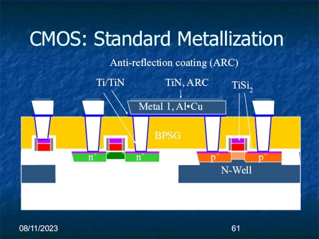
CMOS: Standard Metallization
P-wafer
N-Well
P-Well
STI
n+
n+
USG
p+
p+
Metal 1, Al•Cu
BPSG
W
P-epi
TiSi2
TiN, ARC
Ti/TiN
Anti-reflection coating (ARC)
08/11/2023
CMOS: Standard Metallization
P-wafer
N-Well
P-Well
STI
n+
n+
USG
p+
p+
Metal 1, Al•Cu
BPSG
W
P-epi
TiSi2
TiN, ARC
Ti/TiN
Anti-reflection coating (ARC)
Слайд 6208/11/2023
Fluorosilicate glass (FSG) is a low-k dielectric (FSG) is a low-k dielectric used in between copper metal layers (FSG)
08/11/2023
Fluorosilicate glass (FSG) is a low-k dielectric (FSG) is a low-k dielectric used in between copper metal layers (FSG)
Слайд 6308/11/2023
Shallow trench isolation (STI), also known as Box Isolation Technique, is an integrated circuit, is
08/11/2023
Shallow trench isolation (STI), also known as Box Isolation Technique, is an integrated circuit, is
Слайд 6408/11/2023
W Plug and TiN/Ti Barrier/Adhesion Layer
08/11/2023
W Plug and TiN/Ti Barrier/Adhesion Layer
Слайд 6508/11/2023
Copper Metallization
08/11/2023
Copper Metallization
Слайд 6608/11/2023
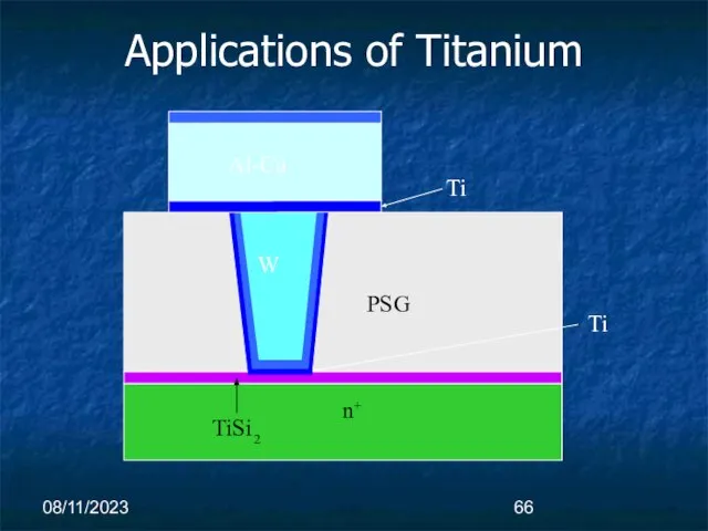
Applications of Titanium
Ti
PSG
TiSi
2
n
+
Ti
W
Al-Cu
08/11/2023
Applications of Titanium
Ti
PSG
TiSi
2
n
+
Ti
W
Al-Cu
Слайд 6708/11/2023
PSG
TiSi2
n
+
TiN, PVD
W
Al-Cu
TiN ARC, PVD
Three Applications of TiN
08/11/2023
PSG
TiSi2
n
+
TiN, PVD
W
Al-Cu
TiN ARC, PVD
Three Applications of TiN
Слайд 6808/11/2023
Aluminum (Al) and gold (Au) are among the most widely employed metals
08/11/2023
Aluminum (Al) and gold (Au) are among the most widely employed metals
Слайд 6908/11/2023
One such example is the use of Au micromechanical switches for RF
08/11/2023
One such example is the use of Au micromechanical switches for RF
Слайд 7008/11/2023
http://airccse.com/eeij/papers/1114eeij03.pdf
Electrical Engineering: An International Journal (EEIJ), Vol. 1, No. 1, June 2014
A
08/11/2023
http://airccse.com/eeij/papers/1114eeij03.pdf
Electrical Engineering: An International Journal (EEIJ), Vol. 1, No. 1, June 2014
A
Слайд 7108/11/2023
Unfortunately, these devices suffer (страдают) from insertion losses and poor electrical solation.
08/11/2023
Unfortunately, these devices suffer (страдают) from insertion losses and poor electrical solation.
Слайд 7208/11/2023
The trilayer cantilever structure was chosen to minimize the deleterious effects of
08/11/2023
The trilayer cantilever structure was chosen to minimize the deleterious effects of
Слайд 7308/11/2023
The processing steps proved to be completely compatible with GaAs substrates.
The released
08/11/2023
The processing steps proved to be completely compatible with GaAs substrates.
The released
Слайд 7408/11/2023
In a second example from RF MEMS, Chang et al. reported the
08/11/2023
In a second example from RF MEMS, Chang et al. reported the
Слайд 7508/11/2023
Each switch is comprised of a series of linked bimorph cantilevers designed
08/11/2023
Each switch is comprised of a series of linked bimorph cantilevers designed
Слайд 7608/11/2023
The released switches were relatively slow, at 10ms, but an actuation voltage
08/11/2023
The released switches were relatively slow, at 10ms, but an actuation voltage
Слайд 7708/11/2023
The reversible phase change allows the shape-memory effect to be used as
08/11/2023
The reversible phase change allows the shape-memory effect to be used as
Слайд 7808/11/2023
Titanium-nickel (TiNi) is among the most popular of the shape-memory alloys, owing
08/11/2023
Titanium-nickel (TiNi) is among the most popular of the shape-memory alloys, owing
Слайд 7908/11/2023
In this study, TiNi films were deposited by co-sputtering elemental Ti and
08/11/2023
In this study, TiNi films were deposited by co-sputtering elemental Ti and
 Операции по техническому обслуживанию оборудования для первичной обработки, хранения и транспортирования молока
 Любовь и дружба в жизни и поэзии Михаила Юрьевича Лермонтова
 Состав ПК Компьютерная система
 Организация и вооружение подразделений Сухопутных войск. Виды вооруженных сил, рода войск
 Фонда поддержки малого предпринимательства городского поселения "Город Краснокаменск"
 Страховые пенсии
 СОЦИОНИЧЕСКИЙ ПОДХОД К ПРОБЛЕМАМ ШКОЛЫ
 С Новым 2022 годом!
 Прием искусства коллаж
 Медиаинформационная грамотность современного педагога
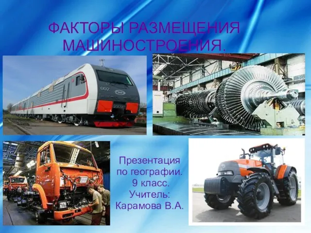 Факторы размещения машиностроения
 Конструирование поясной одежды
 Томмазо ди Джованни ди Симоне Кассаи по прозвищу Мазаччо
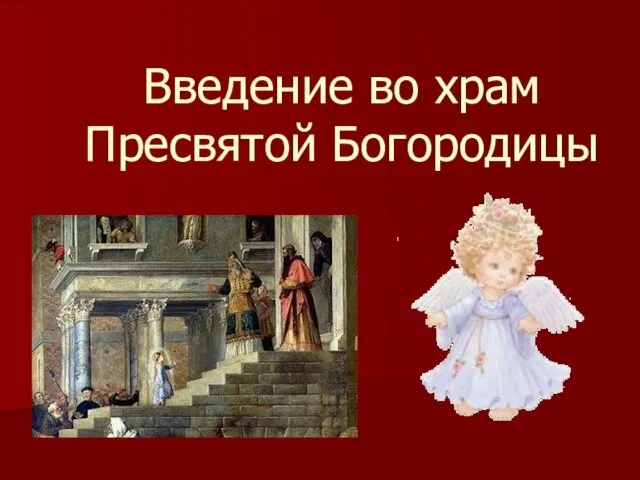 Введение во храм Пресвятой Богородицы
 Парки моего округа
 Государственная (итоговая) аттестация обучающихся общеобразовательных учрежденийКемеровской области
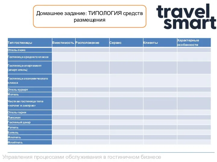 Типология средств размещения
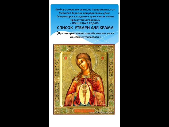 Список утвари для храма
 Приемы быстрого счета
 Коммерческое предложение
 Памятка держателя карты ПАО Сбербанк
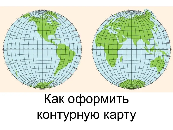 Презентация к уроку географии _Правила заполнения контурной карты_
 Изучение нумерации
 离心风机安装技术交底
 Методика обучения библиотекаря созданию электронных таблиц в программе MS Excel
 Общепринятые форматы листов бумаги
 РА Медиастарз ( весь спектр интернет рекламы) 10 лет назад мы были первыми!
 Экономика