- Система питания ноутбука

Содержание
- 2. Целевая аудитория Все электротехники, такие как: PE, TE, FAE, CSD Необходимые знания Электронные схемы Цифровые логические
- 3. 1.1 Введение в NB системы питания 1.2 Последовательность питания и управления 2.1 Блок-схема цепей питания 2.2
- 4. Как мы знаем, ноутбук питание обеспечивается адаптерами (19V) или батарей (14.8V). Тем не менее, различные (不同
- 5. 1.1 NB (Yuhina) power system : AUX Power PWM Charger P-MOS SI4425 P-MOS SI4425 PWM MAX1999
- 6. 1.1 NB (Yuhina) power system : S5 Power PWM MAX1645 Charger P-MOS SI4425 P-MOS SI4425 PWM
- 7. 1.1 NB (Yuhina) power system : S3 Power PWM MAX1645 Charger P-MOS SI4425 P-MOS SI4425 PWM
- 8. PWM MAX1645 Charger P-MOS SI4425 P-MOS SI4425 PWM MAX1999 PWM MAX1715 AD+ N-MOS FD9412 N-MOS FD9412
- 9. Почему мы должны различать тип питания среди (在 ... 之中) AUX, S5, S3, S0? Как мы
- 10. AUX Power S5 Power S3 Power S0 Power BAT only AD+ or AUX_S5 3D3V_S5 1D5V_S5 DCBATOUT
- 11. DCBATOUT a. Когда батарея или адаптер подключен в (插入), DCBATOUT будет вводить питание в MAX1999 контактный
- 12. Сигнал AC_IN потянули, когда адаптер был вставлен. Мощность по логике вывода MAX1999_SD, чтобы вызвать 3D3V_S5. В
- 13. When MAX1999 – Pin 3(ON3) pull hi, the 3D3V_S5 will be turn on. b. Circuit operation
- 14. When AC_IN is HI, The MOS-U13 will be turned on, and 3D3V_LAN_S5 will be generated. This
- 15. When the power button was pressed, south bridge will pull hi the PM_SLP_S4#, and 5V_S3 power
- 16. 3D3V_S3 power is generated by U25 N-MOS from 3D3V_S5 when PM_SLP_S4# is hi . Hi Hi
- 17. When 5V_S3 power was building, MAX1715 pin – 11 is pulled hi, and 2D5V_S3 will be
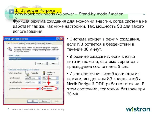
- 18. Функция режима ожидания для экономии энергии, когда система не работает так же, как ниже настройки. Так,
- 19. After PM_SLP_S4# signal was generated for a few μ sec , the South Bridge will output
- 20. PM_SLP_S3# signal is also used to turn on 5V、3D3V、2D5V_S0. b. Circuit operation – 5V,3D3V,&2D5V_S0 :
- 21. -- P4 CPU_ VCO power – architecture : PWM MAX1546 CPU LDO CM2843 Phase 1 Power
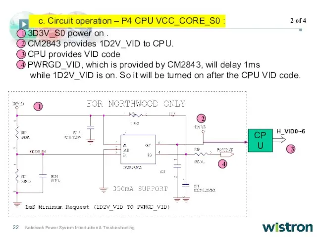
- 22. 3D3V_S0 power on . CM2843 provides 1D2V_VID to CPU. CPU provides VID code PWRGD_VID, which is
- 23. 4 5 3 5 1 1 2 1 MAX1546 Power is ready . CM1843 generates 1D2V_VID
- 24. The step-down circuit starts working as soon as the switch signal begins. The VCC_CORE is produced
- 25. PWM MAX1546 ISL6218 CPU LDO CM2843 Phase 1 Power module Phase 2 Power module Phase 3
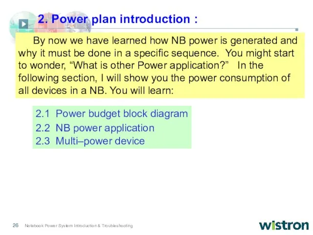
- 26. By now we have learned how NB power is generated and why it must be done
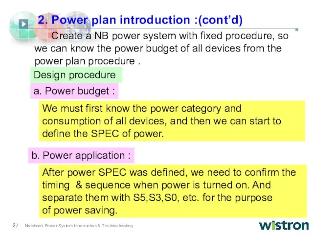
- 27. Create a NB power system with fixed procedure, so we can know the power budget of
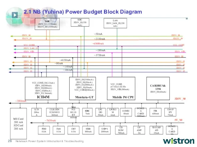
- 28. 1D25V_S0 VCC_CORE_S0(2.5mA ) 1D5V_S0(599mA) 3D3V_S0(480mA ) 1D5V_S5(90mA ) 3D3V_S5( 166mA) ICH4M VCC_CORE 1D5V_S0(3140mA ) 3D3V_S0(20mA )
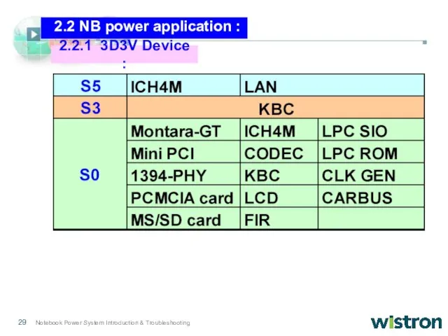
- 29. 2.2.1 3D3V Device : 2.2 NB power application :
- 30. 2.2.3 2D5V Device : 2.2.2 5V Device :
- 31. 2.2.6 1D2V_VID Device : 2.2.5 1D25V Device : 2.2.7 VCC_CORE Device : 2.2.4 1D5V Device :
- 32. 2.3 Multi-power device :
- 33. No power means when the power button is pressed, the power LED is not turned on,
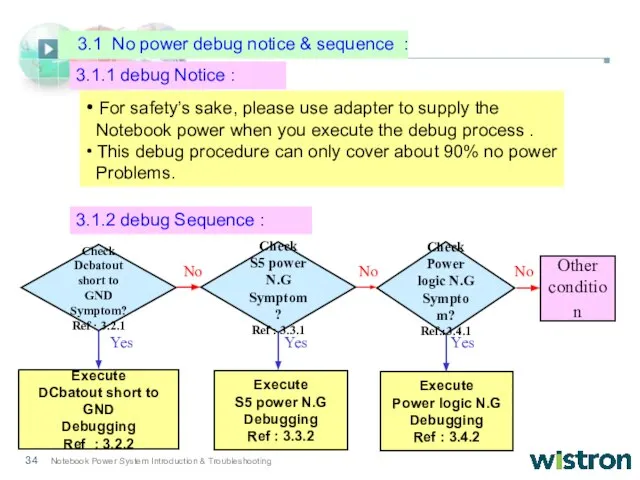
- 34. 3.1.1 debug Notice : • For safety’s sake, please use adapter to supply the Notebook power
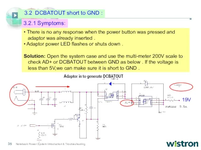
- 35. 3.2.1 Symptoms: • There is no any response when the power button was pressed and adaptor
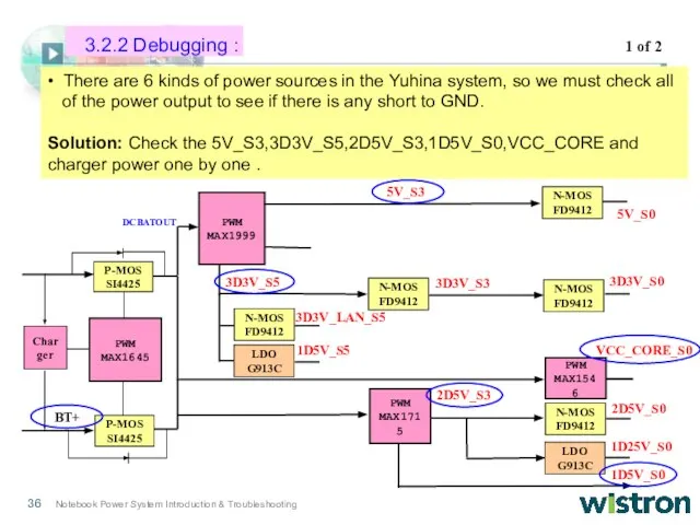
- 36. • There are 6 kinds of power sources in the Yuhina system, so we must check
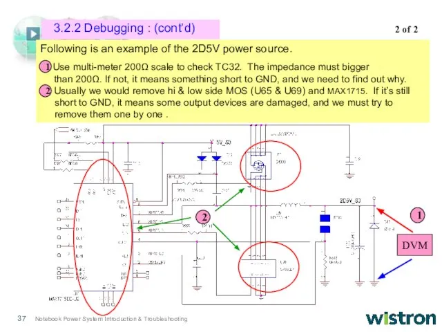
- 37. Following is an example of the 2D5V power source. Use multi-meter 200Ω scale to check TC32.
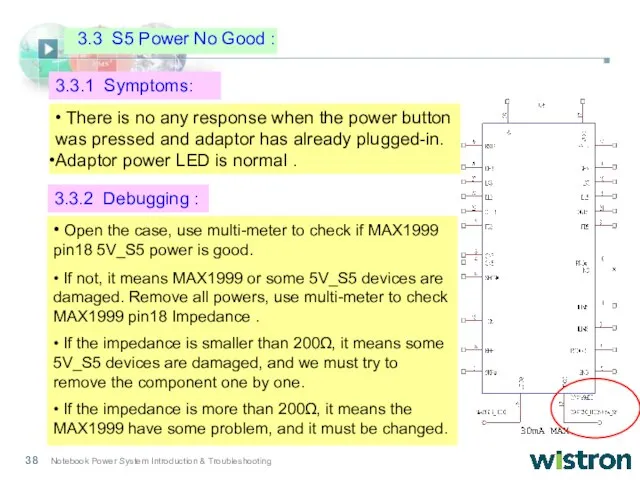
- 38. 3.3.1 Symptoms: • There is no any response when the power button was pressed and adaptor
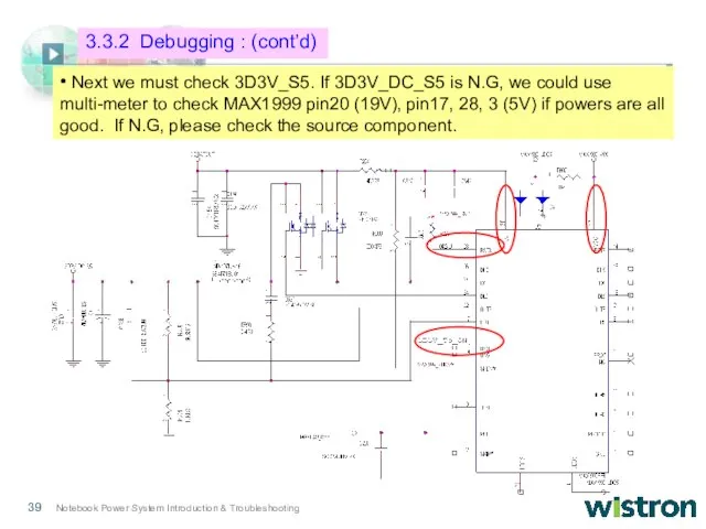
- 39. • Next we must check 3D3V_S5. If 3D3V_DC_S5 is N.G, we could use multi-meter to check
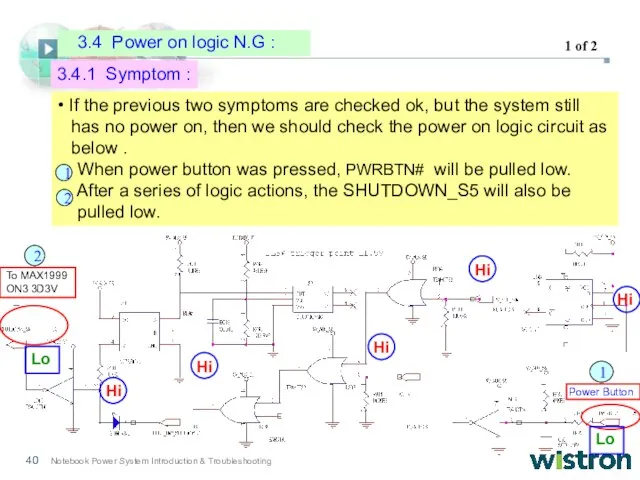
- 40. 3.4.1 Symptom : • If the previous two symptoms are checked ok, but the system still
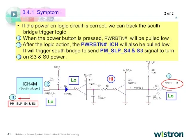
- 41. • If the power on logic circuit is correct, we can track the south bridge trigger
- 43. Скачать презентацию
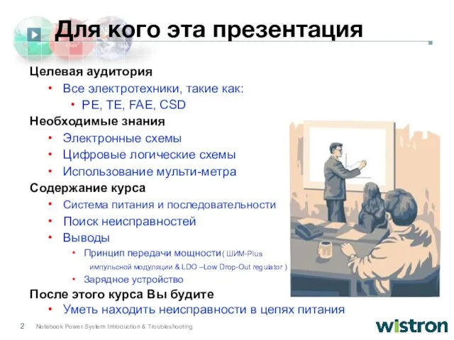
Слайд 2Целевая аудитория
Все электротехники, такие как:
PE, TE, FAE, CSD
Необходимые знания
Электронные
Целевая аудитория
Все электротехники, такие как:
PE, TE, FAE, CSD
Необходимые знания
Электронные
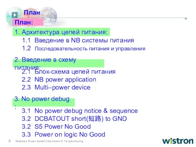
Слайд 3 1.1 Введение в NB системы питания
1.2 Последовательность питания и управления
2.1
1.1 Введение в NB системы питания
1.2 Последовательность питания и управления
2.1
Слайд 4 Как мы знаем, ноутбук питание обеспечивается адаптерами (19V) или батарей (14.8V).
Как мы знаем, ноутбук питание обеспечивается адаптерами (19V) или батарей (14.8V).
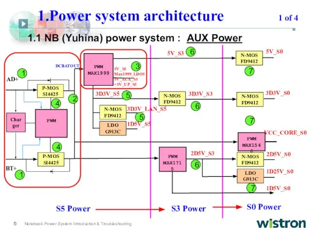
Слайд 5 1.1 NB (Yuhina) power system : AUX Power
PWM
Charger
P-MOS
SI4425
P-MOS
SI4425
PWM
MAX1999
PWM
MAX1715
AD+
BT+
N-MOS
FD9412
N-MOS
FD9412
N-MOS
FD9412
N-MOS
FD9412
5V_S5
Max1999_LDO5
5V_AUX_S5
+5V_UP_S5
3D3V_S5
DCBATOUT
N-MOS
FD9412
LDO
G913C
5V_S3
3D3V_S3
5V_S0
3D3V_S0
3D3V_LAN_S5
1D5V_S5
2D5V_S3
2D5V_S0
LDO
G913C
1D25V_S0
S5 Power
S3 Power
S0
1.1 NB (Yuhina) power system : AUX Power
PWM
Charger
P-MOS
SI4425
P-MOS
SI4425
PWM
MAX1999
PWM
MAX1715
AD+
BT+
N-MOS
FD9412
N-MOS
FD9412
N-MOS
FD9412
N-MOS
FD9412
5V_S5
Max1999_LDO5
5V_AUX_S5
+5V_UP_S5
3D3V_S5
DCBATOUT
N-MOS
FD9412
LDO
G913C
5V_S3
3D3V_S3
5V_S0
3D3V_S0
3D3V_LAN_S5
1D5V_S5
2D5V_S3
2D5V_S0
LDO
G913C
1D25V_S0
S5 Power
S3 Power
S0
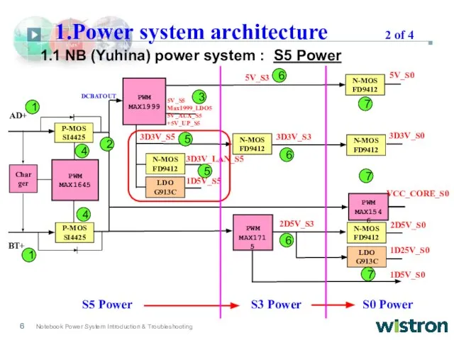
Слайд 6 1.1 NB (Yuhina) power system : S5 Power
PWM
MAX1645
Charger
P-MOS
SI4425
P-MOS
SI4425
PWM
MAX1999
PWM
MAX1715
AD+
BT+
N-MOS
FD9412
N-MOS
FD9412
N-MOS
FD9412
N-MOS
FD9412
5V_S5
Max1999_LDO5
5V_AUX_S5
+5V_UP_S5
3D3V_S5
DCBATOUT
N-MOS
FD9412
LDO
G913C
5V_S3
3D3V_S3
5V_S0
3D3V_S0
3D3V_LAN_S5
1D5V_S5
2D5V_S3
2D5V_S0
LDO
G913C
1D25V_S0
S5 Power
S3 Power
S0 Power
PWM
MAX1546
VCC_CORE_S0
1D5V_S0
1
4
3
2
1
6
6
5
7
6
4
7
7
5
1.Power
1.1 NB (Yuhina) power system : S5 Power
PWM
MAX1645
Charger
P-MOS
SI4425
P-MOS
SI4425
PWM
MAX1999
PWM
MAX1715
AD+
BT+
N-MOS
FD9412
N-MOS
FD9412
N-MOS
FD9412
N-MOS
FD9412
5V_S5
Max1999_LDO5
5V_AUX_S5
+5V_UP_S5
3D3V_S5
DCBATOUT
N-MOS
FD9412
LDO
G913C
5V_S3
3D3V_S3
5V_S0
3D3V_S0
3D3V_LAN_S5
1D5V_S5
2D5V_S3
2D5V_S0
LDO
G913C
1D25V_S0
S5 Power
S3 Power
S0 Power
PWM
MAX1546
VCC_CORE_S0
1D5V_S0
1
4
3
2
1
6
6
5
7
6
4
7
7
5
1.Power
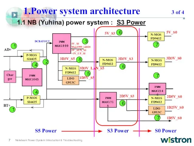
Слайд 7 1.1 NB (Yuhina) power system : S3 Power
PWM
MAX1645
Charger
P-MOS
SI4425
P-MOS
SI4425
PWM
MAX1999
PWM
MAX1715
AD+
N-MOS
FD9412
N-MOS
FD9412
N-MOS
FD9412
N-MOS
FD9412
5V_S5
Max1999_LDO5
5V_AUX_S5
+5V_UP_S5
3D3V_S5
DCBATOUT
N-MOS
FD9412
LDO
G913C
5V_S3
3D3V_S3
5V_S0
3D3V_S0
3D3V_LAN_S5
1D5V_S5
2D5V_S3
2D5V_S0
LDO
G913C
1D25V_S0
S5 Power
S3 Power
S0 Power
PWM
MAX1546
1D5V_S0
1
4
3
2
1
6
6
5
7
6
4
7
7
5
BT+
1.Power
1.1 NB (Yuhina) power system : S3 Power
PWM
MAX1645
Charger
P-MOS
SI4425
P-MOS
SI4425
PWM
MAX1999
PWM
MAX1715
AD+
N-MOS
FD9412
N-MOS
FD9412
N-MOS
FD9412
N-MOS
FD9412
5V_S5
Max1999_LDO5
5V_AUX_S5
+5V_UP_S5
3D3V_S5
DCBATOUT
N-MOS
FD9412
LDO
G913C
5V_S3
3D3V_S3
5V_S0
3D3V_S0
3D3V_LAN_S5
1D5V_S5
2D5V_S3
2D5V_S0
LDO
G913C
1D25V_S0
S5 Power
S3 Power
S0 Power
PWM
MAX1546
1D5V_S0
1
4
3
2
1
6
6
5
7
6
4
7
7
5
BT+
1.Power
Слайд 8PWM
MAX1645
Charger
P-MOS
SI4425
P-MOS
SI4425
PWM
MAX1999
PWM
MAX1715
AD+
N-MOS
FD9412
N-MOS
FD9412
N-MOS
FD9412
N-MOS
FD9412
5V_S5
Max1999_LDO5
5V_AUX_S5
+5V_UP_S5
3D3V_S5
DCBATOUT
N-MOS
FD9412
LDO
G913C
5V_S3
3D3V_S3
5V_S0
3D3V_S0
3D3V_LAN_S5
1D5V_S5
2D5V_S3
2D5V_S0
LDO
G913C
1D25V_S0
S5 Power
S3 Power
S0 Power
PWM
MAX1546
1D5V_S0
1
4
3
2
1
6
6
5
7
6
4
7
7
5
BT+
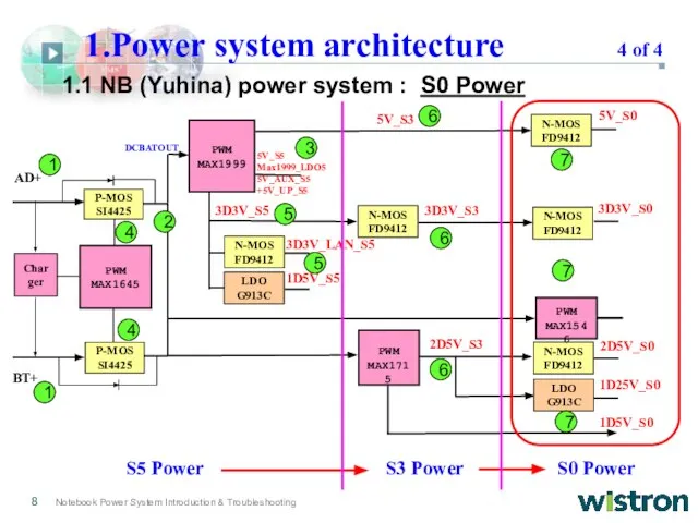
1.1 NB (Yuhina) power system : S0 Power
1.Power
PWM
MAX1645
Charger
P-MOS
SI4425
P-MOS
SI4425
PWM
MAX1999
PWM
MAX1715
AD+
N-MOS
FD9412
N-MOS
FD9412
N-MOS
FD9412
N-MOS
FD9412
5V_S5
Max1999_LDO5
5V_AUX_S5
+5V_UP_S5
3D3V_S5
DCBATOUT
N-MOS
FD9412
LDO
G913C
5V_S3
3D3V_S3
5V_S0
3D3V_S0
3D3V_LAN_S5
1D5V_S5
2D5V_S3
2D5V_S0
LDO
G913C
1D25V_S0
S5 Power
S3 Power
S0 Power
PWM
MAX1546
1D5V_S0
1
4
3
2
1
6
6
5
7
6
4
7
7
5
BT+
1.1 NB (Yuhina) power system : S0 Power
1.Power
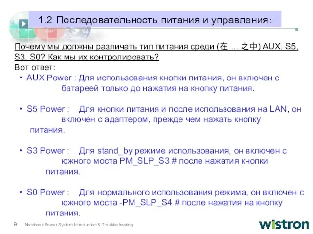
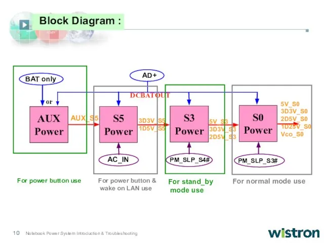
Слайд 9Почему мы должны различать тип питания среди (在 ... 之中) AUX, S5,
S3,
S3,
Слайд 10AUX
Power
S5
Power
S3
Power
S0
Power
BAT only
AD+
or
AUX_S5
3D3V_S5
1D5V_S5
DCBATOUT
AC_IN
PM_SLP_S4#
PM_SLP_S3#
5V_S3
3D3V_S3
2D5V_S3
5V_S0
3D3V_S0
2D5V_S0
1D25V_S0
Vco_S0
For power button use
For stand_by
mode use
For normal mode use
For power
AUX
Power
S5
Power
S3
Power
S0
Power
BAT only
AD+
or
AUX_S5
3D3V_S5
1D5V_S5
DCBATOUT
AC_IN
PM_SLP_S4#
PM_SLP_S3#
5V_S3
3D3V_S3
2D5V_S3
5V_S0
3D3V_S0
2D5V_S0
1D25V_S0
Vco_S0
For power button use
For stand_by
mode use
For normal mode use
For power
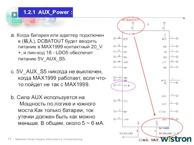
Слайд 11DCBATOUT
a. Когда батарея или адаптер подключен в (插入), DCBATOUT будет вводить
DCBATOUT
a. Когда батарея или адаптер подключен в (插入), DCBATOUT будет вводить
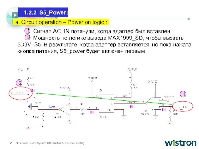
Слайд 12 Сигнал AC_IN потянули, когда адаптер был вставлен.
Мощность по логике вывода
Сигнал AC_IN потянули, когда адаптер был вставлен.
Мощность по логике вывода
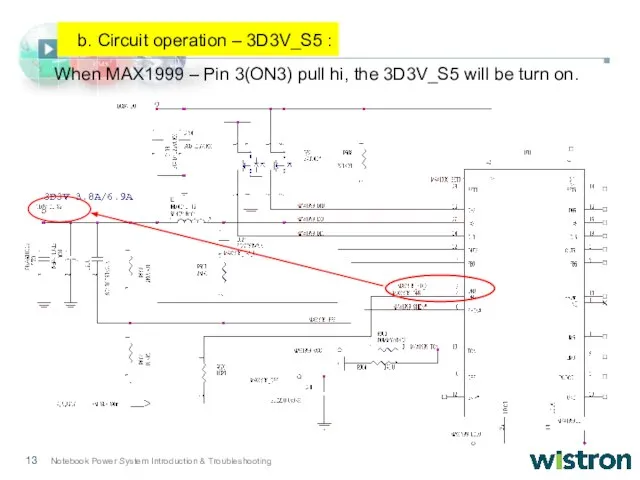
Слайд 13 When MAX1999 – Pin 3(ON3) pull hi, the 3D3V_S5 will be
When MAX1999 – Pin 3(ON3) pull hi, the 3D3V_S5 will be
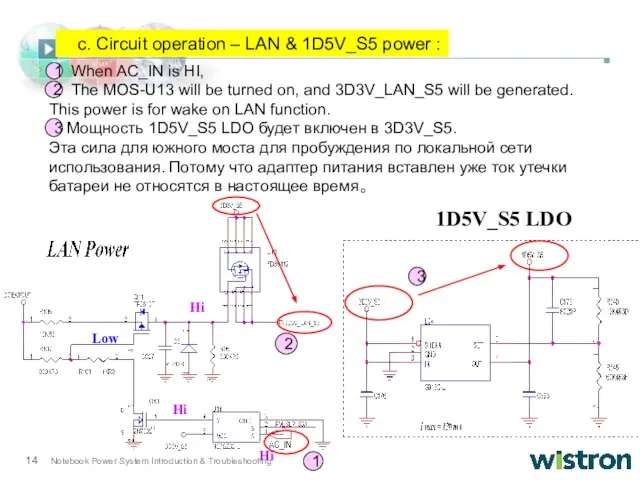
Слайд 14 When AC_IN is HI,
The MOS-U13 will be turned on,
When AC_IN is HI,
The MOS-U13 will be turned on,
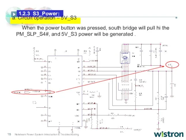
Слайд 15 When the power button was pressed, south bridge will pull hi
When the power button was pressed, south bridge will pull hi
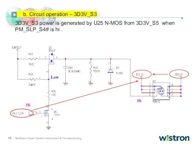
Слайд 163D3V_S3 power is generated by U25 N-MOS from 3D3V_S5 when PM_SLP_S4# is
3D3V_S3 power is generated by U25 N-MOS from 3D3V_S5 when PM_SLP_S4# is
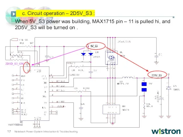
Слайд 17When 5V_S3 power was building, MAX1715 pin – 11 is pulled hi,
When 5V_S3 power was building, MAX1715 pin – 11 is pulled hi,
Слайд 18Функция режима ожидания для экономии энергии, когда система не работает так же,
Функция режима ожидания для экономии энергии, когда система не работает так же,
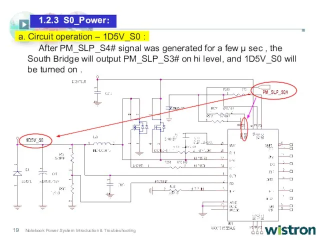
Слайд 19 After PM_SLP_S4# signal was generated for a few μ sec ,
After PM_SLP_S4# signal was generated for a few μ sec ,
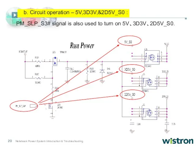
Слайд 20PM_SLP_S3# signal is also used to turn on 5V、3D3V、2D5V_S0.
b. Circuit operation –
PM_SLP_S3# signal is also used to turn on 5V、3D3V、2D5V_S0.
b. Circuit operation –
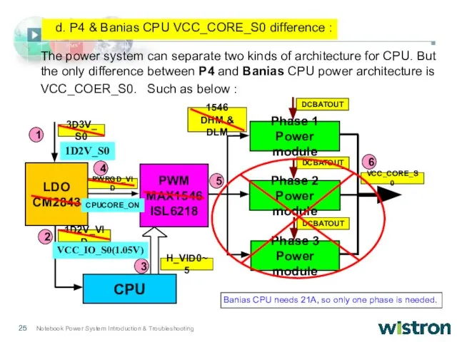
Слайд 21 -- P4 CPU_ VCO power – architecture :
PWM
MAX1546
CPU
LDO
CM2843
Phase 1
Power module
Phase 2
Power
-- P4 CPU_ VCO power – architecture :
PWM
MAX1546
CPU
LDO
CM2843
Phase 1
Power module
Phase 2
Power
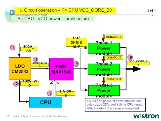
Слайд 22 3D3V_S0 power on .
CM2843 provides 1D2V_VID to CPU.
CPU provides
3D3V_S0 power on .
CM2843 provides 1D2V_VID to CPU.
CPU provides
Слайд 234
5
3
5
1
1
2
1
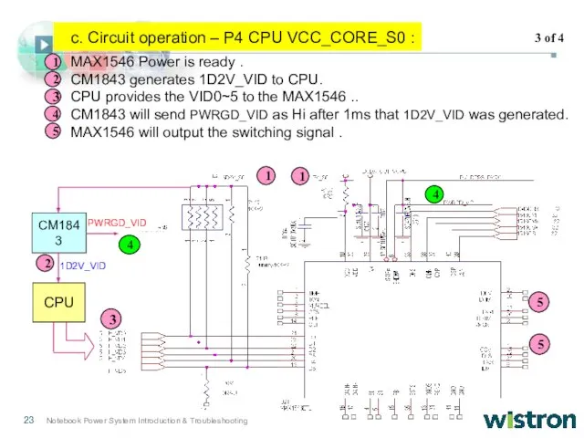
MAX1546 Power is ready .
CM1843 generates 1D2V_VID to CPU.
CPU provides the VID0~5
4
5
3
5
1
1
2
1
MAX1546 Power is ready .
CM1843 generates 1D2V_VID to CPU.
CPU provides the VID0~5
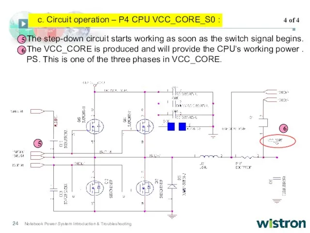
Слайд 24The step-down circuit starts working as soon as the switch signal begins.
The
The step-down circuit starts working as soon as the switch signal begins.
The
Слайд 25PWM
MAX1546
ISL6218
CPU
LDO
CM2843
Phase 1
Power module
Phase 2
Power module
Phase 3
Power module
3D3V_S0
1D2V_VID
H_VID0~5
DCBATOUT
DCBATOUT
DCBATOUT
VCC_CORE_S0
PWRGD_VID
1
5
4
3
2
1546
DHM & DLM
6
1D2V_S0
VCC_IO_S0(1.05V)
CPUCORE_ON
Banias CPU needs 21A,
PWM
MAX1546
ISL6218
CPU
LDO
CM2843
Phase 1
Power module
Phase 2
Power module
Phase 3
Power module
3D3V_S0
1D2V_VID
H_VID0~5
DCBATOUT
DCBATOUT
DCBATOUT
VCC_CORE_S0
PWRGD_VID
1
5
4
3
2
1546
DHM & DLM
6
1D2V_S0
VCC_IO_S0(1.05V)
CPUCORE_ON
Banias CPU needs 21A,
Слайд 26 By now we have learned how NB power is generated and
By now we have learned how NB power is generated and
Слайд 27 Create a NB power system with fixed procedure, so we can
Create a NB power system with fixed procedure, so we can
Слайд 281D25V_S0
VCC_CORE_S0(2.5mA )
1D5V_S0(599mA)
3D3V_S0(480mA )
1D5V_S5(90mA )
3D3V_S5( 166mA)
ICH4M
VCC_CORE
1D5V_S0(3140mA )
3D3V_S0(20mA )
2D5V_S3(2000mA )
2D5V_S0(50mA)
VCC_CORE(940mA )
Montara-GT
Mobile P4 CPU
3D3V_S3
VCC_CORE
(67.4A)-3.2G
1D25V_S0
VCC_CORE_S0(2.5mA )
1D5V_S0(599mA)
3D3V_S0(480mA )
1D5V_S5(90mA )
3D3V_S5( 166mA)
ICH4M
VCC_CORE
1D5V_S0(3140mA )
3D3V_S0(20mA )
2D5V_S3(2000mA )
2D5V_S0(50mA)
VCC_CORE(940mA )
Montara-GT
Mobile P4 CPU
3D3V_S3
VCC_CORE
(67.4A)-3.2G
Слайд 292.2.1 3D3V Device :
2.2 NB power application :
2.2.1 3D3V Device :
2.2 NB power application :
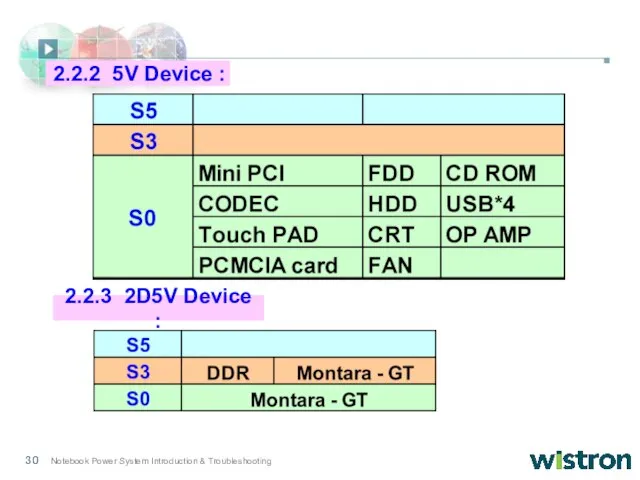
Слайд 302.2.3 2D5V Device :
2.2.2 5V Device :
2.2.3 2D5V Device :
2.2.2 5V Device :
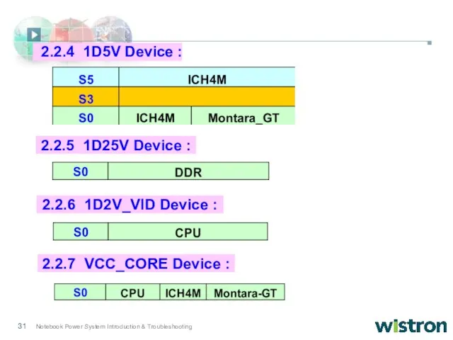
Слайд 312.2.6 1D2V_VID Device :
2.2.5 1D25V Device :
2.2.7 VCC_CORE Device :
2.2.4 1D5V Device
2.2.6 1D2V_VID Device :
2.2.5 1D25V Device :
2.2.7 VCC_CORE Device :
2.2.4 1D5V Device
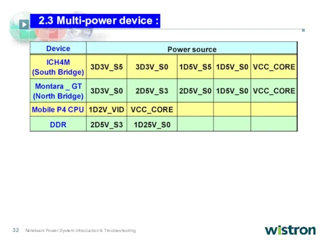
Слайд 322.3 Multi-power device :
2.3 Multi-power device :
Слайд 33 No power means when the power button is pressed, the power
No power means when the power button is pressed, the power
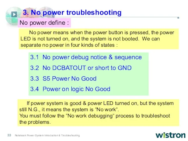
Слайд 343.1.1 debug Notice :
• For safety’s sake, please use adapter to supply
3.1.1 debug Notice :
• For safety’s sake, please use adapter to supply
Слайд 353.2.1 Symptoms:
• There is no any response when the power button was
3.2.1 Symptoms:
• There is no any response when the power button was
Слайд 36• There are 6 kinds of power sources in the Yuhina system,
• There are 6 kinds of power sources in the Yuhina system,
Слайд 37Following is an example of the 2D5V power source.
Use multi-meter 200Ω
Following is an example of the 2D5V power source.
Use multi-meter 200Ω
Слайд 38
3.3.1 Symptoms:
• There is no any response when the power button
3.3.1 Symptoms:
• There is no any response when the power button
Слайд 39• Next we must check 3D3V_S5. If 3D3V_DC_S5 is N.G, we could
• Next we must check 3D3V_S5. If 3D3V_DC_S5 is N.G, we could
Слайд 403.4.1 Symptom :
• If the previous two symptoms are checked ok, but
3.4.1 Symptom :
• If the previous two symptoms are checked ok, but
Слайд 41• If the power on logic circuit is correct, we can track
• If the power on logic circuit is correct, we can track
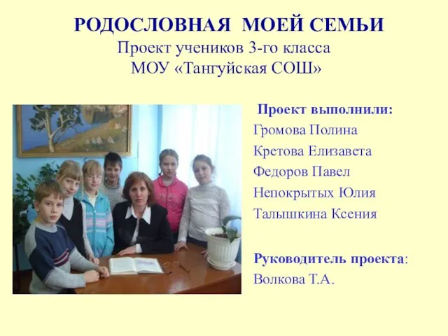 Родословная моей семьи
 Рубцова Ирина Алексеевнаучитель ТСОШ 1. Прочитать параграф учебника и найти ответ на вопрос. Самостоятельная работа с книгой.
 Культурное наследие Сибири
  Л Кривые второго порядка
 мужчины и женщины - такие похожие и такие разные?
 Тропический и внетропический циклоны
 Презентация на тему Пластиковая посуда и опасность для здоровья школьника
 Соцсети для e-commerce Уголок экспериментальной торговли
 Презентация на тему Опыт по определению диаметра молекулы
  Nutzen USB
 Северокавказский букварь как транслятор советской идеологии: 1927–1932 годы (на материалах редфонда ДГПБ)
 Единицы массы. Тонна. Центнер (4 класс)
 Rock & Roll
 Добрый день, мы приветствуем Вас на экскурсии по Древнему Риму!
 ПСИХОФИЗИОЛОГИЧЕСКИЙ ДИАГНОСТИЧЕСКИЙ КОМПЛЕКС «ФОБОС»®
 ИКТ-инфраструктура
 Школа ППМИ – 2022. Старт приоритетного регионального проекта Наш выбор
 Атака на короля при разных видах рокировки
 Теорема Пифагора. 8 класс
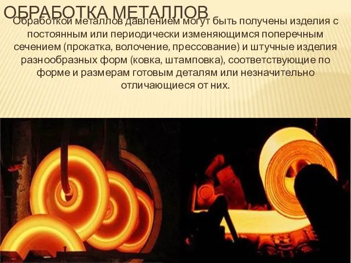 Обработка металлов
 Светлое воскресение христово
 ПОРТФОЛИОучителя физики
 Поезд в Пушкинские горы. Проект создания трансферного узла
 Учет договоров ДОУ в новой версии системы ИС-ПРО 7.07
 Мониторинг и управление инфраструктурой ИТ на комплексных объектах ТЭК
 Школа Блогеров
 Ребусы
 Волонтерский отряд«Исток»