- Metal-Insulator-Semiconductor and Metal-Insulator-Metal Structures. Part II

Содержание
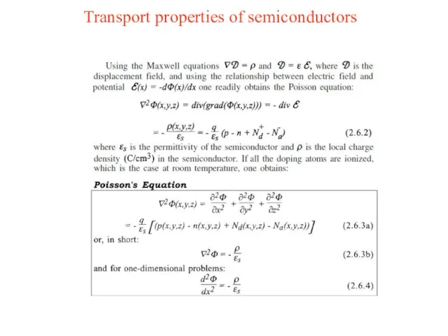
- 2. Transport properties of semiconductors
- 3. Transport properties of semiconductors
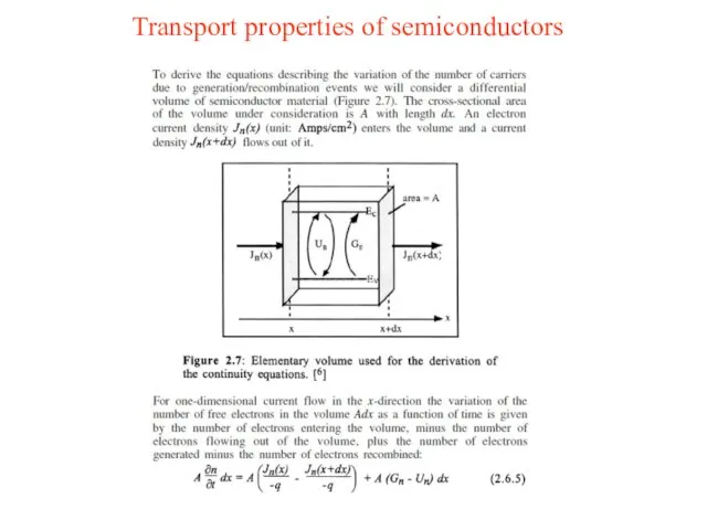
- 4. Transport properties of semiconductors
- 5. Transport properties of semiconductors
- 6. Transport properties of semiconductors
- 7. Transport properties of semiconductors
- 8. Transport properties of semiconductors
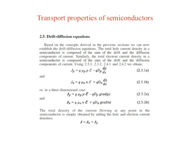
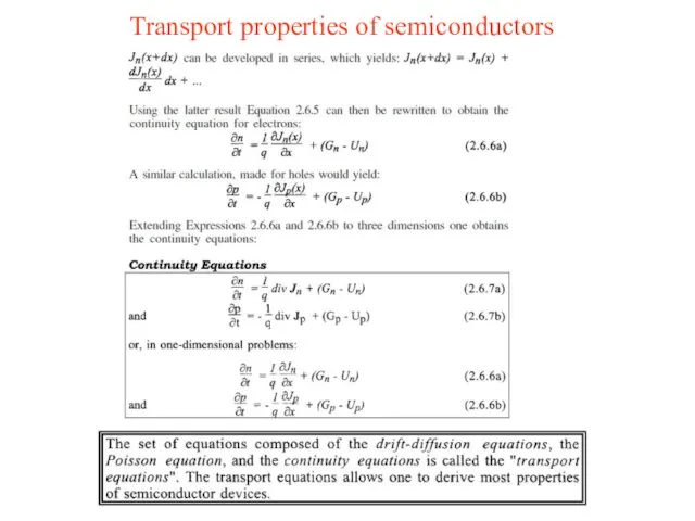
- 9. Transport properties of semiconductors
- 10. Transport properties of semiconductors
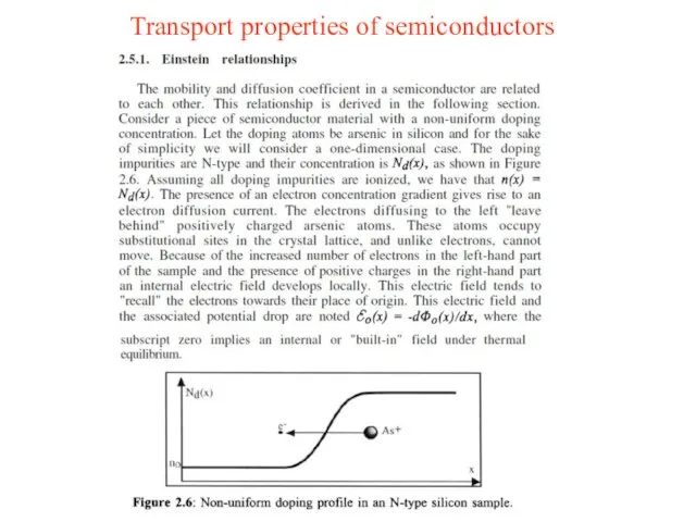
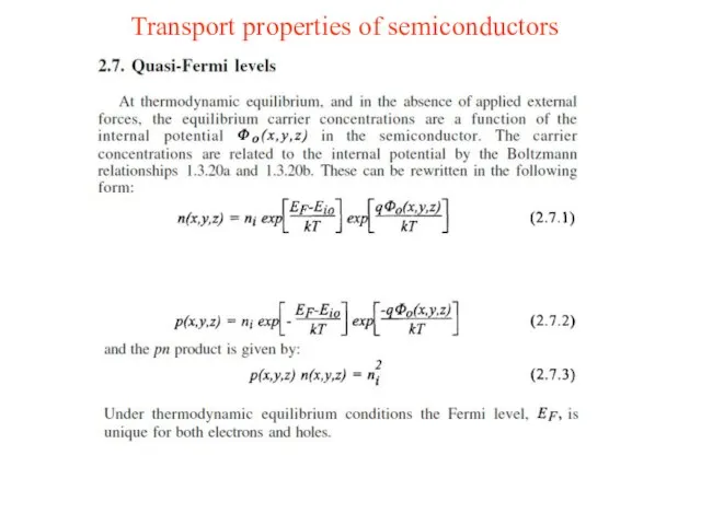
- 11. Transport properties of semiconductors
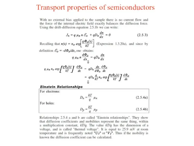
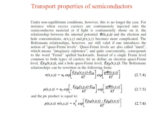
- 12. Transport properties of semiconductors
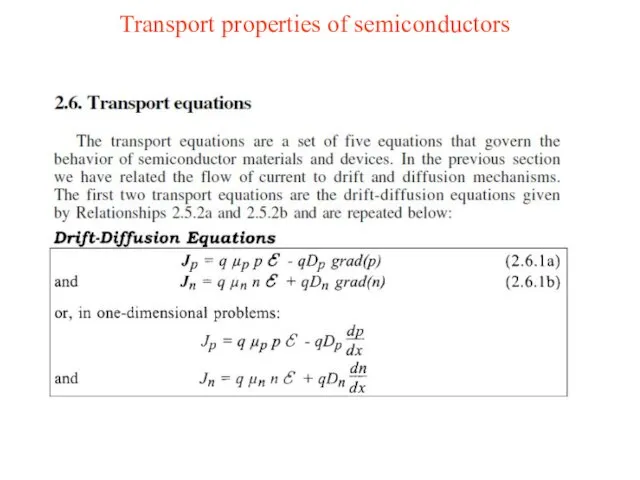
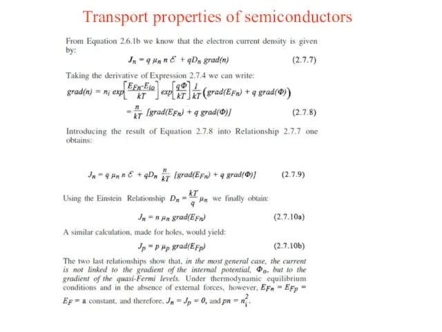
- 13. Transport properties of semiconductors
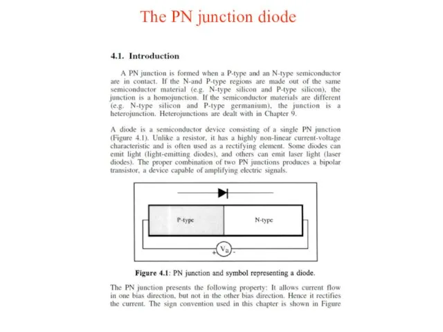
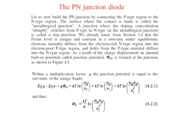
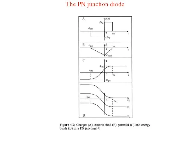
- 14. The PN junction diode
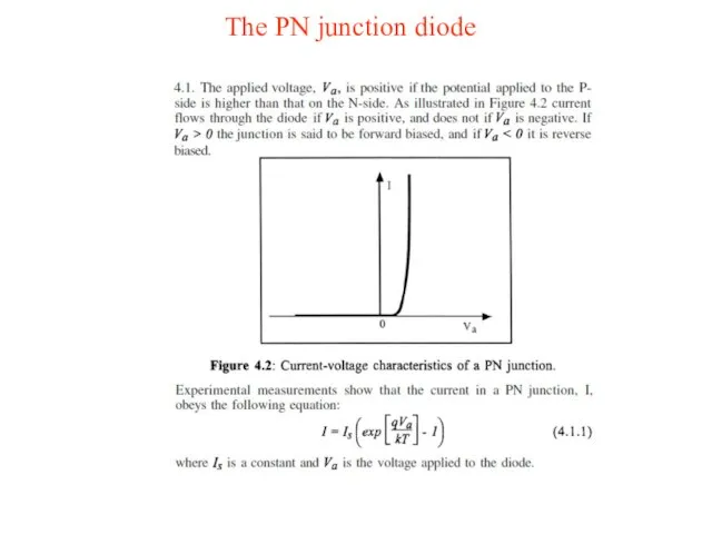
- 15. The PN junction diode
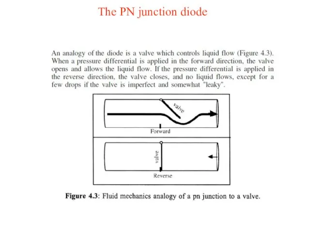
- 16. The PN junction diode
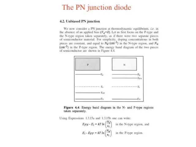
- 17. The PN junction diode
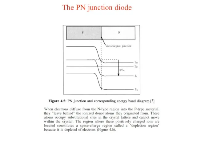
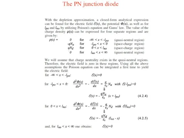
- 18. The PN junction diode
- 19. The PN junction diode
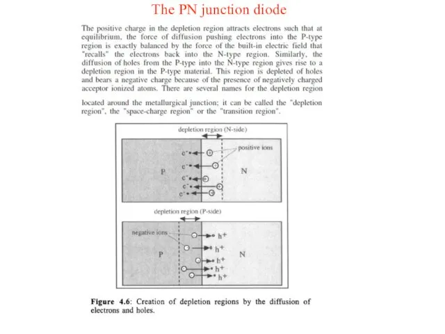
- 20. The PN junction diode
- 21. The PN junction diode
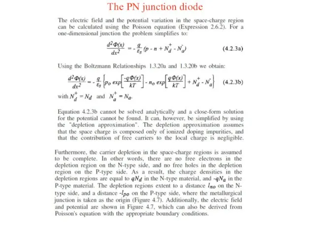
- 22. The PN junction diode
- 23. The PN junction diode
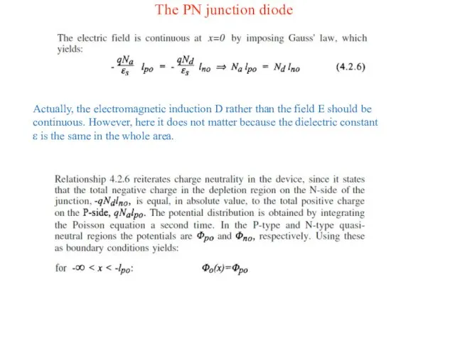
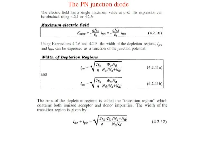
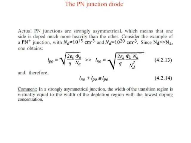
- 24. The PN junction diode Actually, the electromagnetic induction D rather than the field E should be
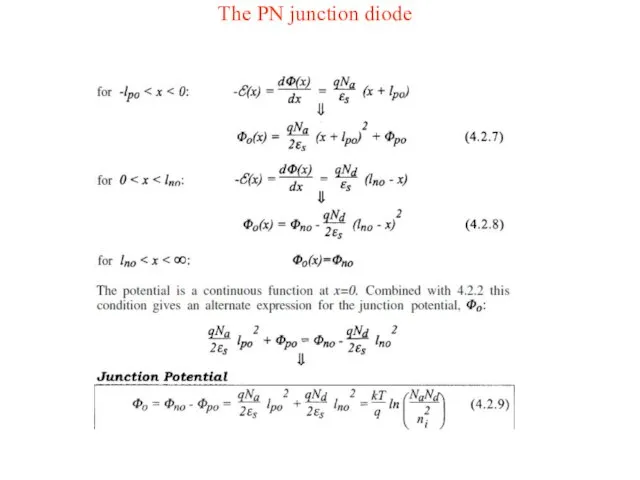
- 25. The PN junction diode
- 26. The PN junction diode
- 27. The PN junction diode
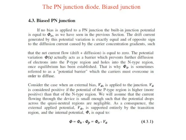
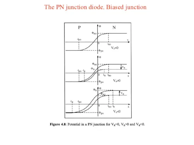
- 28. The PN junction diode. Biased junction
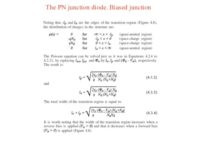
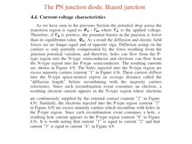
- 29. The PN junction diode. Biased junction
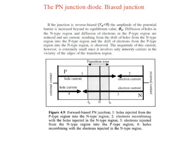
- 30. The PN junction diode. Biased junction
- 31. The PN junction diode. Biased junction
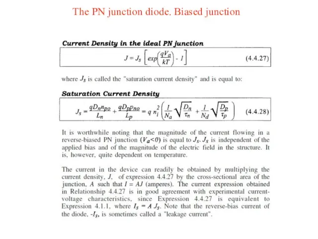
- 32. The PN junction diode. Biased junction
- 33. The PN junction diode. Biased junction
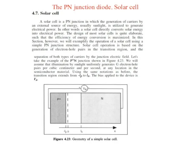
- 34. The PN junction diode. Solar cell
- 36. Скачать презентацию
Слайд 3Transport properties of semiconductors
Transport properties of semiconductors
Слайд 4Transport properties of semiconductors
Transport properties of semiconductors
Слайд 5Transport properties of semiconductors
Transport properties of semiconductors
Слайд 6Transport properties of semiconductors
Transport properties of semiconductors
Слайд 7Transport properties of semiconductors
Transport properties of semiconductors
Слайд 8Transport properties of semiconductors
Transport properties of semiconductors
Слайд 9Transport properties of semiconductors
Transport properties of semiconductors
Слайд 10Transport properties of semiconductors
Transport properties of semiconductors
Слайд 11Transport properties of semiconductors
Transport properties of semiconductors
Слайд 12Transport properties of semiconductors
Transport properties of semiconductors
Слайд 13Transport properties of semiconductors
Transport properties of semiconductors
Слайд 14The PN junction diode
The PN junction diode
Слайд 15The PN junction diode
The PN junction diode
Слайд 16The PN junction diode
The PN junction diode
Слайд 17The PN junction diode
The PN junction diode
Слайд 18The PN junction diode
The PN junction diode
Слайд 19The PN junction diode
The PN junction diode
Слайд 20The PN junction diode
The PN junction diode
Слайд 21The PN junction diode
The PN junction diode
Слайд 22The PN junction diode
The PN junction diode
Слайд 23The PN junction diode
The PN junction diode
Слайд 24The PN junction diode
Actually, the electromagnetic induction D rather than the field
The PN junction diode
Actually, the electromagnetic induction D rather than the field
Слайд 25The PN junction diode
The PN junction diode
Слайд 26The PN junction diode
The PN junction diode
Слайд 27The PN junction diode
The PN junction diode
Слайд 28The PN junction diode. Biased junction
The PN junction diode. Biased junction
Слайд 29The PN junction diode. Biased junction
The PN junction diode. Biased junction
Слайд 30The PN junction diode. Biased junction
The PN junction diode. Biased junction
Слайд 31The PN junction diode. Biased junction
The PN junction diode. Biased junction
Слайд 32The PN junction diode. Biased junction
The PN junction diode. Biased junction
Слайд 33The PN junction diode. Biased junction
The PN junction diode. Biased junction
Слайд 34The PN junction diode. Solar cell
The PN junction diode. Solar cell
 London
 Основы менеджмента
 Кто покупает? Портрет вашего клиента
 Презентация на тему Непрерывные случайные величины
 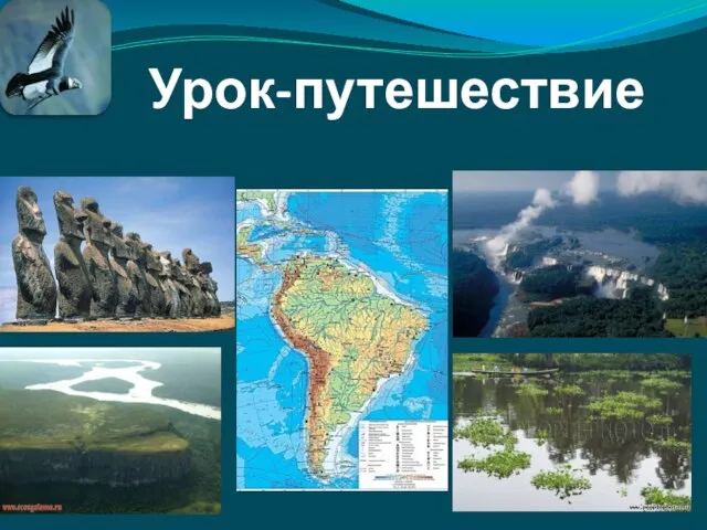 Урок-путешествие
 Экспортная Интернет площадка www.exim.uz
 Неправительственные правозащитные организации
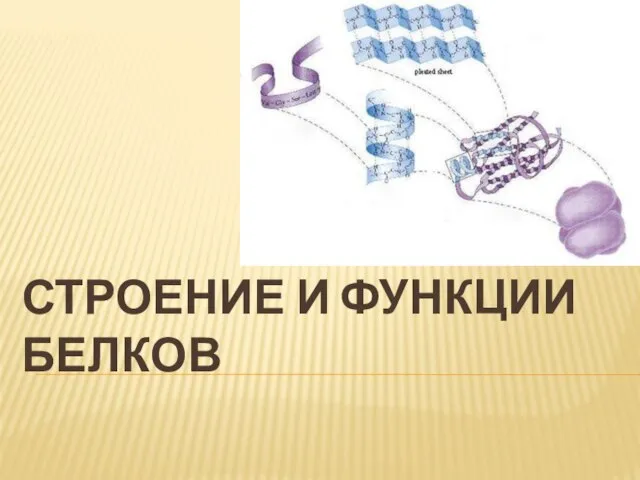 Презентация на тему Строение и функции белков
  Инвестиционные программы Gold Fort
 Артюхова Нина Михайловна — русская детская писательница
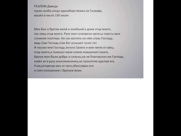 Особо избранный чин 33-х псалмов вечнозаветной псалтири на святорусском языке
 Продажа земельных участков. Республика Крым
 Презентация на тему Ромео и Джульетта
 Филогенетический и онтогенетический методы развития психики живых существ
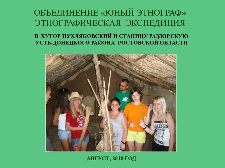 Место проведения экспедиции
 project-presentation-template
 Медиаобразованиев России www.edu.of.ru/mediaeducation
 Тема: Правописание частиц НЕ и НИ.
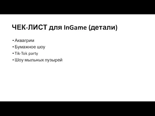 Чек-лист для InGame (детали)
 Презентация на тему Всеволод Александрович Рождественский 29 марта 1895- 31 августа 1977
 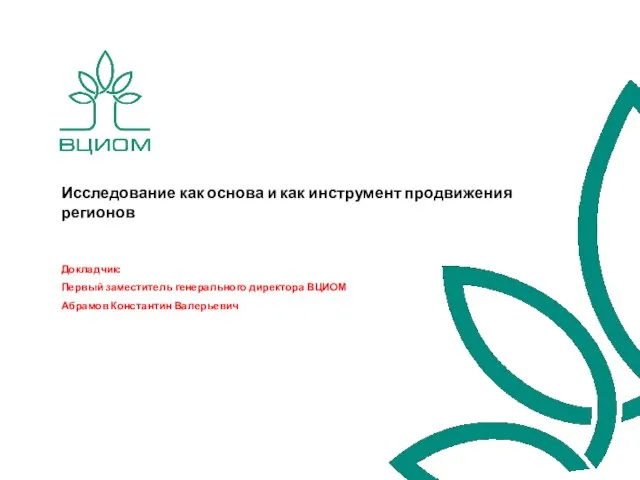 Исследование как основа и как инструмент продвижения регионов
 Мир на рубеже веков
 Решение задач (Практическое пособие)
 Тема:«Адаптационный период в 5б классе»Классный руководитель: Триколе О.В.
 Элемент архитектуры портал
 Переніс слві
 Задание по дисциплине Маркетинговые стратегии
 Ведение бизнеса по обслуживанию граждан пожилого возраста и инвалидов