- slides topic

Содержание
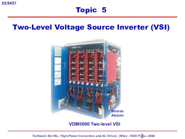
- 2. VDM5000 Two-level VSI Topic 5 Two-Level Voltage Source Inverter (VSI) Source: Alstom
- 3. Sinusoidal PWM Space vector modulation Lecture Topics To control inverter output frequency (fundamental) To control inverter
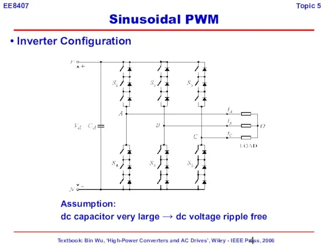
- 4. Inverter Configuration Assumption: dc capacitor very large → dc voltage ripple free Sinusoidal PWM
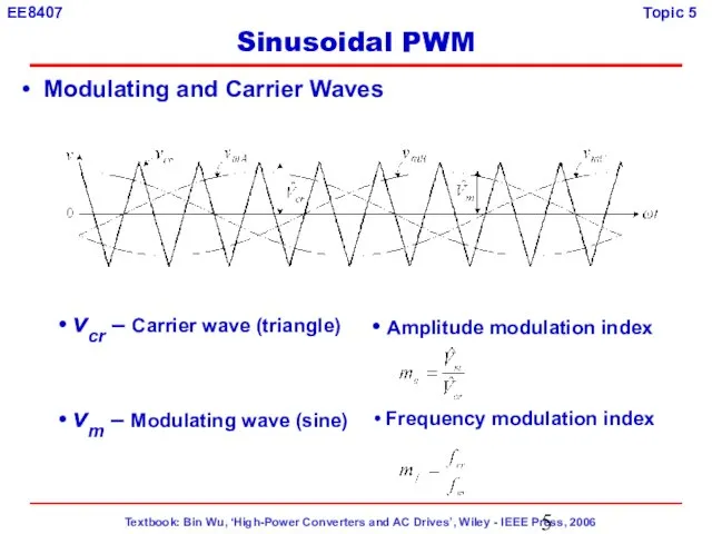
- 5. Modulating and Carrier Waves vcr – Carrier wave (triangle) Amplitude modulation index Frequency modulation index vm
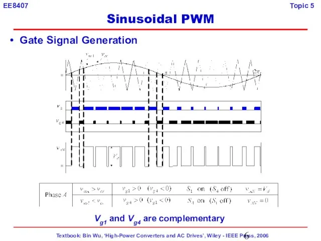
- 6. Gate Signal Generation Vg1 and Vg4 are complementary Sinusoidal PWM
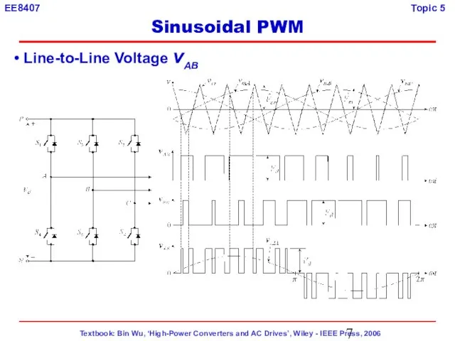
- 7. Line-to-Line Voltage vAB Sinusoidal PWM
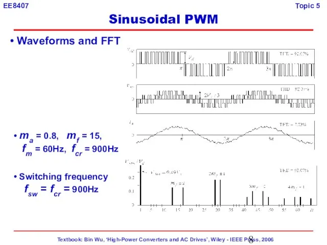
- 8. Waveforms and FFT ma = 0.8, mf = 15, fm = 60Hz, fcr = 900Hz Switching
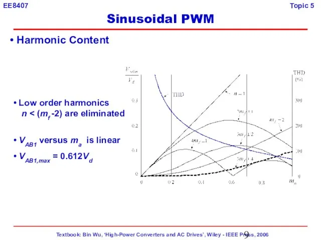
- 9. Harmonic Content Low order harmonics n VAB1 versus ma is linear VAB1,max = 0.612Vd Sinusoidal PWM
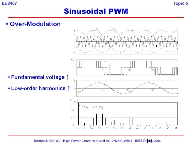
- 10. Over-Modulation Fundamental voltage ↑ Low-order harmonics ↑ Sinusoidal PWM
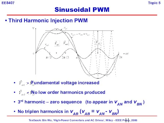
- 11. Third Harmonic Injection PWM - Fundamental voltage increased - No low order harmonics produced 3rd harmonic
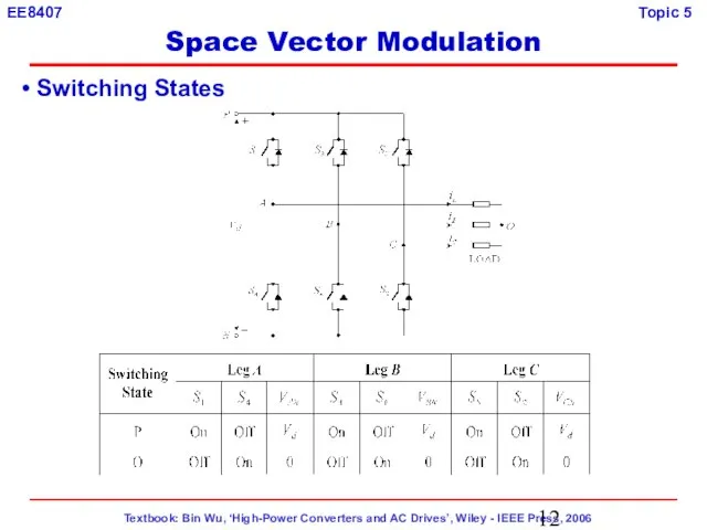
- 12. Switching States Space Vector Modulation
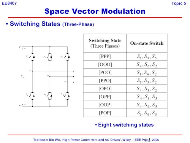
- 13. Switching States (Three-Phase) Eight switching states Space Vector Modulation
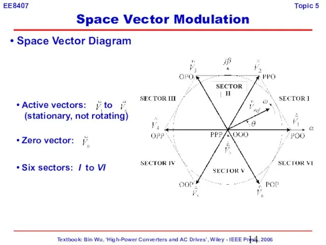
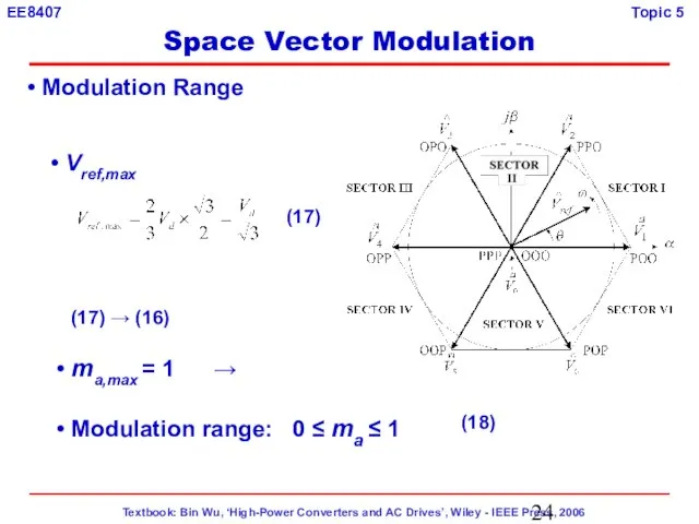
- 14. Space Vector Diagram Active vectors: to (stationary, not rotating) Zero vector: Six sectors: I to VI
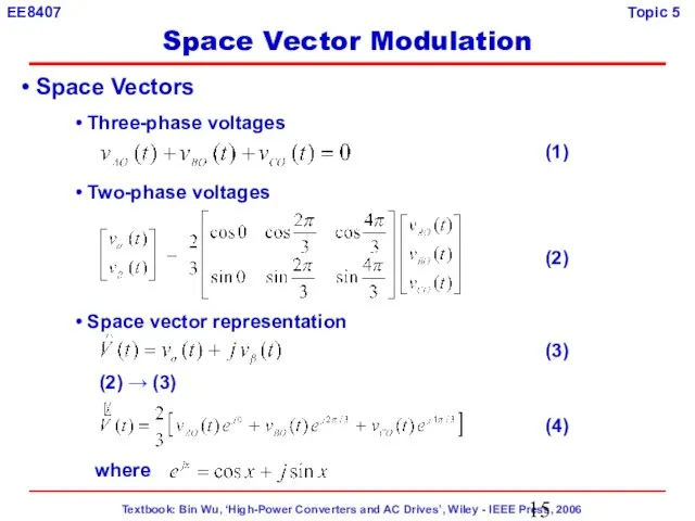
- 15. Space Vectors Three-phase voltages Two-phase voltages Space vector representation (2) → (3) where (3) (1) (2)
- 16. Space Vectors (Example) Switching state [POO] → S1, S6 and S2 ON and (5) → (4)
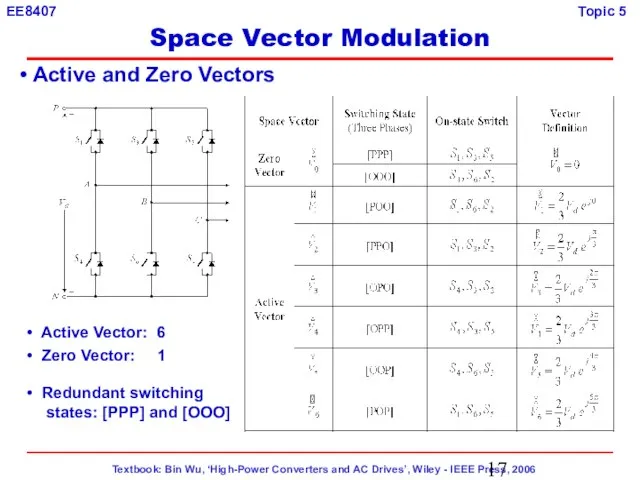
- 17. Active and Zero Vectors Active Vector: 6 Zero Vector: 1 Redundant switching states: [PPP] and [OOO]
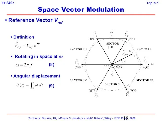
- 18. (8) Reference Vector Vref Definition Angular displacement (9) Rotating in space at ω Space Vector Modulation
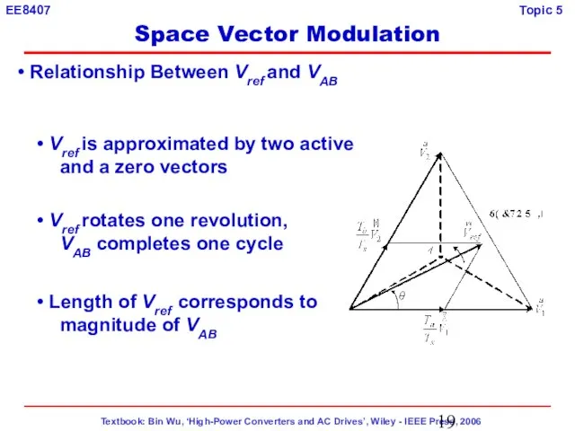
- 19. Relationship Between Vref and VAB Vref is approximated by two active and a zero vectors Vref
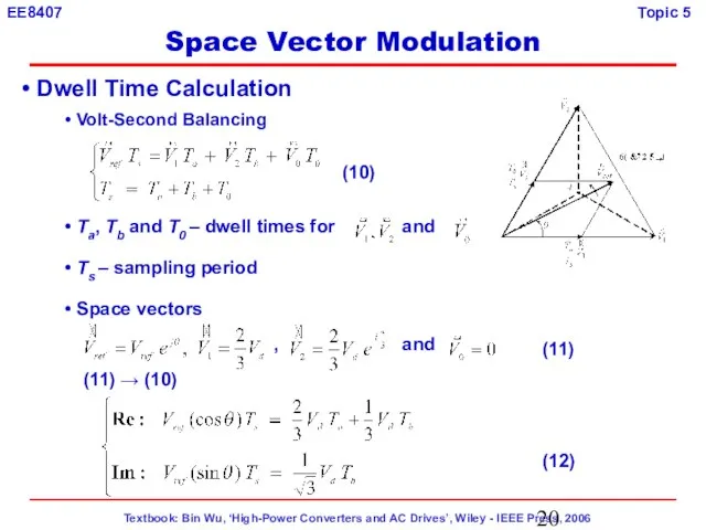
- 20. Dwell Time Calculation Volt-Second Balancing (10) Ta, Tb and T0 – dwell times for and Ts
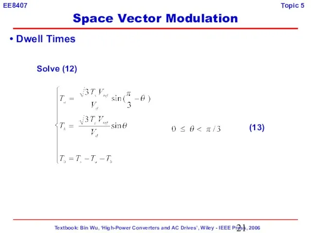
- 21. Dwell Times Solve (12) (13) Space Vector Modulation
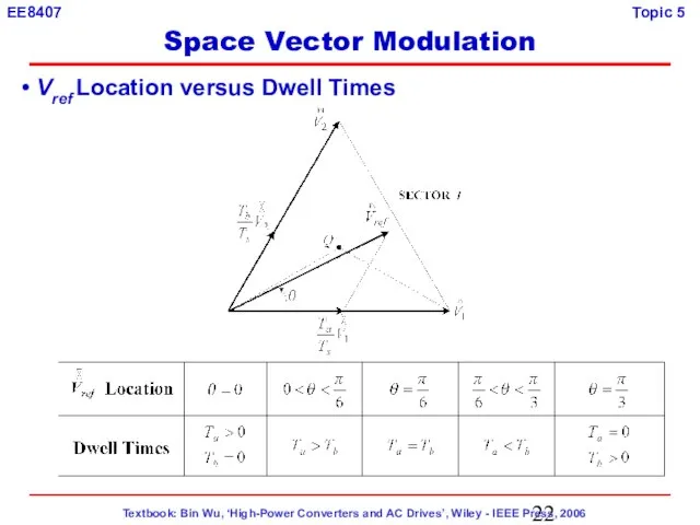
- 22. Vref Location versus Dwell Times Space Vector Modulation
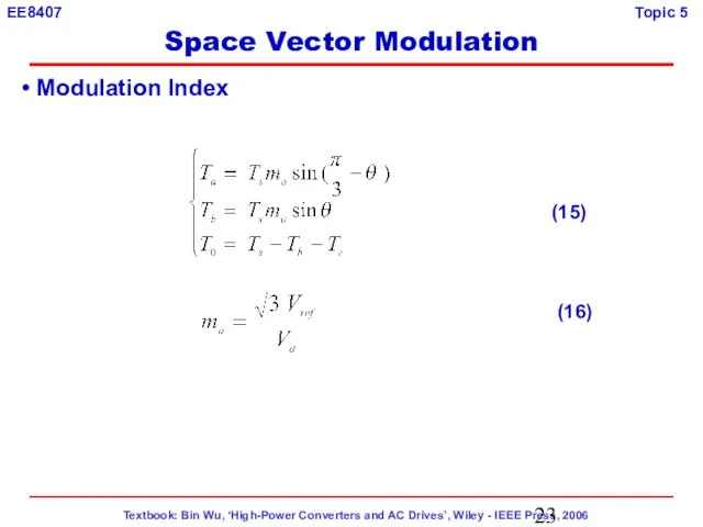
- 23. Modulation Index (15) (16) Space Vector Modulation
- 24. Modulation Range Vref,max (17) (17) → (16) ma,max = 1 → Modulation range: 0 ≤ ma
- 25. Switching Sequence Design Basic Requirement: Minimize the number of switchings per sampling period Ts Implementation: Transition
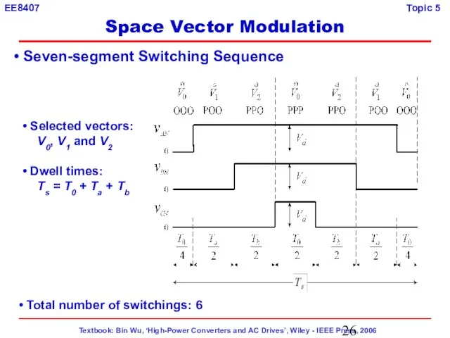
- 26. Seven-segment Switching Sequence Total number of switchings: 6 Selected vectors: V0, V1 and V2 Dwell times:
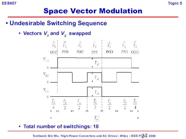
- 27. Undesirable Switching Sequence Vectors V1 and V2 swapped Total number of switchings: 10 Space Vector Modulation
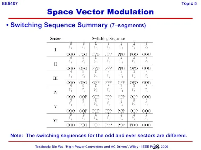
- 28. Switching Sequence Summary (7–segments) Note: The switching sequences for the odd and ever sectors are different.
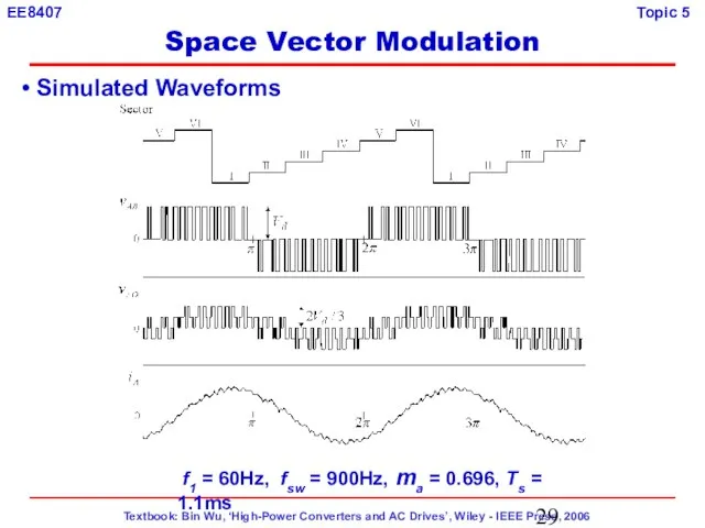
- 29. Simulated Waveforms f1 = 60Hz, fsw = 900Hz, ma = 0.696, Ts = 1.1ms Space Vector
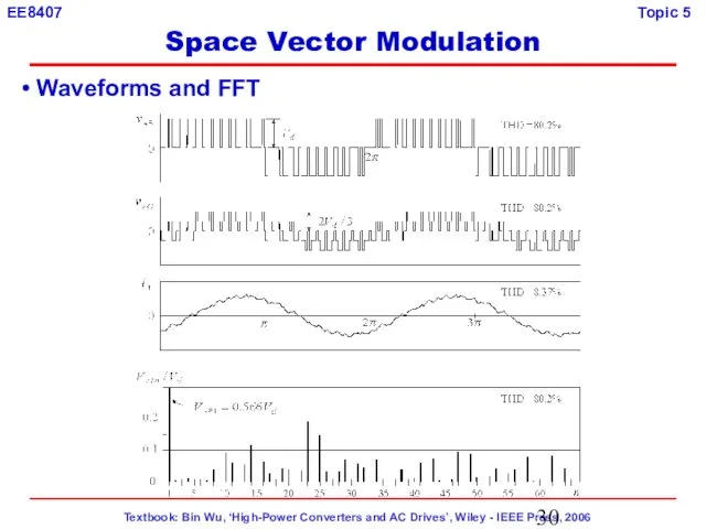
- 30. Waveforms and FFT Space Vector Modulation
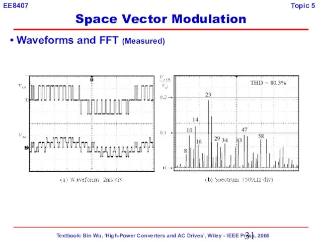
- 31. Waveforms and FFT (Measured) Space Vector Modulation
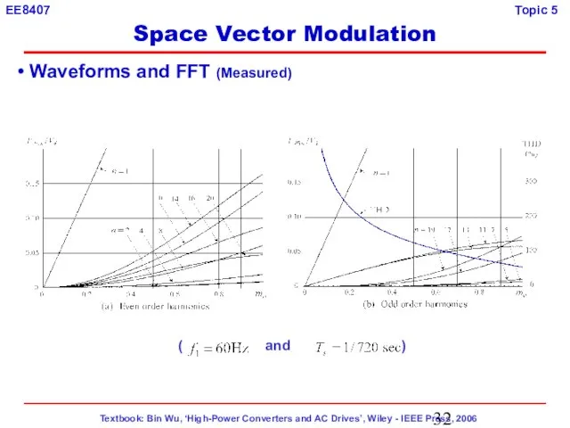
- 32. Waveforms and FFT (Measured) ( and ) Space Vector Modulation
- 33. Even-Order Harmonic Elimination Type-A sequence (starts and ends with [OOO]) Type-B sequence (starts and ends with
- 34. Even-Order Harmonic Elimination Space vector Diagram Space Vector Modulation
- 35. Even-Order Harmonic Elimination Measured waveforms and FFT Space Vector Modulation
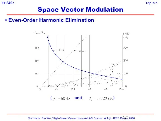
- 36. Even-Order Harmonic Elimination ( and ) Space Vector Modulation
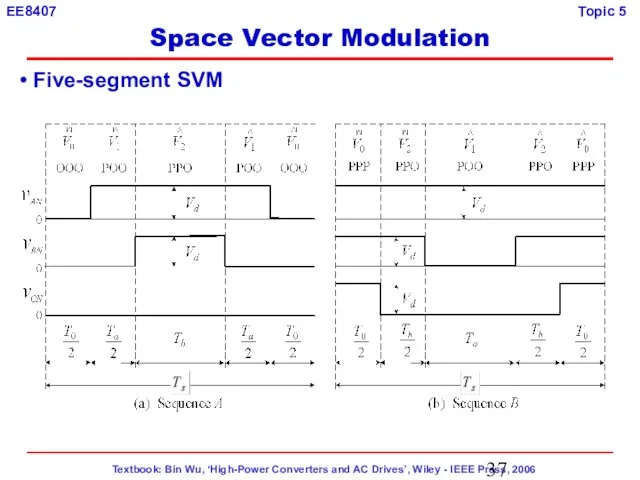
- 37. Five-segment SVM Space Vector Modulation
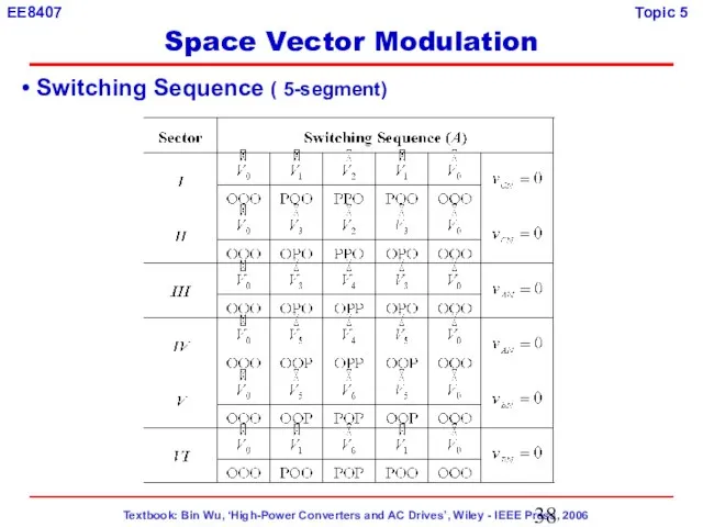
- 38. Switching Sequence ( 5-segment) Space Vector Modulation
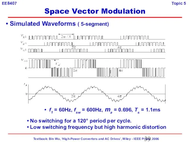
- 39. Simulated Waveforms ( 5-segment) No switching for a 120° period per cycle. Low switching frequency but
- 41. Скачать презентацию
Слайд 3 Sinusoidal PWM
Space vector modulation
Lecture Topics
To control inverter output
Sinusoidal PWM
Space vector modulation
Lecture Topics
To control inverter output
Слайд 4 Inverter Configuration
Assumption:
dc capacitor very large → dc voltage ripple free
Inverter Configuration
Assumption:
dc capacitor very large → dc voltage ripple free
Слайд 5 Modulating and Carrier Waves
vcr – Carrier wave (triangle)
Amplitude modulation
Modulating and Carrier Waves
vcr – Carrier wave (triangle)
Amplitude modulation
Слайд 6 Gate Signal Generation
Vg1 and Vg4 are complementary
Sinusoidal PWM
Gate Signal Generation
Vg1 and Vg4 are complementary
Sinusoidal PWM
Слайд 7 Line-to-Line Voltage vAB
Sinusoidal PWM
Line-to-Line Voltage vAB
Sinusoidal PWM
Слайд 8 Waveforms and FFT
ma = 0.8, mf = 15,
fm
Waveforms and FFT
ma = 0.8, mf = 15,
fm
Слайд 9 Harmonic Content
Low order harmonics
n < (mf -2) are eliminated
Harmonic Content
Low order harmonics
n < (mf -2) are eliminated
Слайд 10 Over-Modulation
Fundamental voltage ↑
Low-order harmonics ↑
Sinusoidal PWM
Over-Modulation
Fundamental voltage ↑
Low-order harmonics ↑
Sinusoidal PWM
Слайд 11 Third Harmonic Injection PWM
- Fundamental voltage increased
- No
Third Harmonic Injection PWM
- Fundamental voltage increased
- No
Слайд 12 Switching States
Space Vector Modulation
Switching States
Space Vector Modulation
Слайд 13 Switching States (Three-Phase)
Eight switching states
Space Vector Modulation
Switching States (Three-Phase)
Eight switching states
Space Vector Modulation
Слайд 14 Space Vector Diagram
Active vectors: to
(stationary, not rotating)
Zero vector:
Space Vector Diagram
Active vectors: to
(stationary, not rotating)
Zero vector:
Слайд 15 Space Vectors
Three-phase voltages
Two-phase voltages
Space vector representation
(2) → (3)
Space Vectors
Three-phase voltages
Two-phase voltages
Space vector representation
(2) → (3)
Слайд 16 Space Vectors (Example)
Switching state [POO] → S1, S6 and S2
Space Vectors (Example)
Switching state [POO] → S1, S6 and S2
![Space Vectors (Example) Switching state [POO] → S1, S6 and S2 ON](/_ipx/f_webp&q_80&fit_contain&s_1440x1080/imagesDir/jpg/381589/slide-15.jpg)
Слайд 17 Active and Zero Vectors
Active Vector: 6
Zero Vector: 1
Redundant
Active and Zero Vectors
Active Vector: 6
Zero Vector: 1
Redundant
Слайд 18(8)
Reference Vector Vref
Definition
Angular displacement
(9)
Rotating in space at
(8)
Reference Vector Vref
Definition
Angular displacement
(9)
Rotating in space at
Слайд 19 Relationship Between Vref and VAB
Vref is approximated by two active
Relationship Between Vref and VAB
Vref is approximated by two active
Слайд 20 Dwell Time Calculation
Volt-Second Balancing
(10)
Ta, Tb and T0 – dwell
Dwell Time Calculation
Volt-Second Balancing
(10)
Ta, Tb and T0 – dwell
Слайд 21 Dwell Times
Solve (12)
(13)
Space Vector Modulation
Dwell Times
Solve (12)
(13)
Space Vector Modulation
Слайд 22 Vref Location versus Dwell Times
Space Vector Modulation
Vref Location versus Dwell Times
Space Vector Modulation
Слайд 23 Modulation Index
(15)
(16)
Space Vector Modulation
Modulation Index
(15)
(16)
Space Vector Modulation
Слайд 24 Modulation Range
Vref,max
(17)
(17) → (16)
ma,max = 1 →
Modulation
Modulation Range
Vref,max
(17)
(17) → (16)
ma,max = 1 →
Modulation
Слайд 25 Switching Sequence Design
Basic Requirement:
Minimize the number of switchings per
Switching Sequence Design
Basic Requirement:
Minimize the number of switchings per
Слайд 26 Seven-segment Switching Sequence
Total number of switchings: 6
Selected vectors:
V0,
Seven-segment Switching Sequence
Total number of switchings: 6
Selected vectors:
V0,
Слайд 27 Undesirable Switching Sequence
Vectors V1 and V2 swapped
Total number of
Undesirable Switching Sequence
Vectors V1 and V2 swapped
Total number of
Слайд 28 Switching Sequence Summary (7–segments)
Note: The switching sequences for the odd and
Switching Sequence Summary (7–segments)
Note: The switching sequences for the odd and
Слайд 29 Simulated Waveforms
f1 = 60Hz, fsw = 900Hz, ma = 0.696,
Simulated Waveforms
f1 = 60Hz, fsw = 900Hz, ma = 0.696,
Слайд 30 Waveforms and FFT
Space Vector Modulation
Waveforms and FFT
Space Vector Modulation
Слайд 31 Waveforms and FFT (Measured)
Space Vector Modulation
Waveforms and FFT (Measured)
Space Vector Modulation
Слайд 32 Waveforms and FFT (Measured)
( and )
Space Vector Modulation
Waveforms and FFT (Measured)
( and )
Space Vector Modulation
Слайд 33 Even-Order Harmonic Elimination
Type-A sequence
(starts and ends with [OOO])
Type-B sequence
Even-Order Harmonic Elimination
Type-A sequence
(starts and ends with [OOO])
Type-B sequence
![Even-Order Harmonic Elimination Type-A sequence (starts and ends with [OOO]) Type-B sequence](/_ipx/f_webp&q_80&fit_contain&s_1440x1080/imagesDir/jpg/381589/slide-32.jpg)
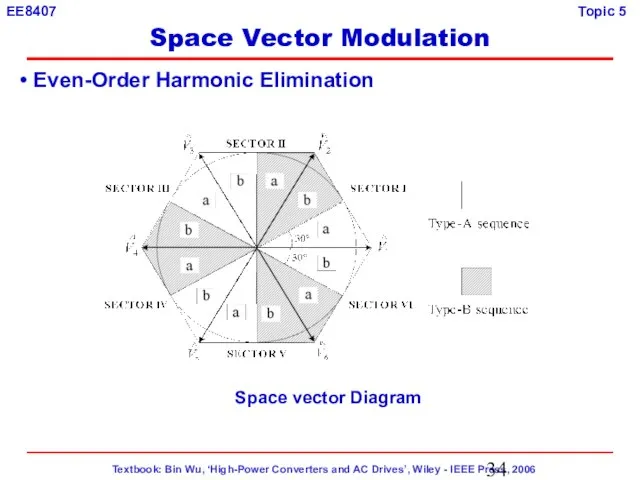
Слайд 34 Even-Order Harmonic Elimination
Space vector Diagram
Space Vector Modulation
Even-Order Harmonic Elimination
Space vector Diagram
Space Vector Modulation
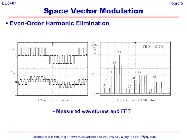
Слайд 35 Even-Order Harmonic Elimination
Measured waveforms and FFT
Space Vector Modulation
Even-Order Harmonic Elimination
Measured waveforms and FFT
Space Vector Modulation
Слайд 36 Even-Order Harmonic Elimination
( and )
Space Vector Modulation
Even-Order Harmonic Elimination
( and )
Space Vector Modulation
Слайд 37 Five-segment SVM
Space Vector Modulation
Five-segment SVM
Space Vector Modulation
Слайд 38 Switching Sequence ( 5-segment)
Space Vector Modulation
Switching Sequence ( 5-segment)
Space Vector Modulation
Слайд 39 Simulated Waveforms ( 5-segment)
No switching for a 120° period per
Simulated Waveforms ( 5-segment)
No switching for a 120° period per
 Конструкт урока
 Презентация на тему Профессия шофер
  Камышинский ХБКТекстильный кластер «Поволжье»
 Совет Существ
 Береги глаза смолоду!
 Диаграмма №1
  Правила сравнения дробей
 Очистка поверхностных вод Минско-Вилейской системы
 Об обучении эсперанто
 Бренд города
 Янтарные штучки
 Обязательные элементы спортивных дисциплин
 Молдавия
 Металлы
 Материалы К заседанию Общественного совета при Федеральной службе по экологическому, технологическому и атомному надзору ПРЕД
 Компания «ФОРМА»ПРЕДСТАВЛЯЕТ…….
 Мировая история: переход к новому времени. Россия в 16-17вв.
 Бизнес-план придорожного отеля Кипарис
 psikhya_Microsoft_PowerPoint
 Партнёрство бизнеса и Даунсайд Ап. Дети с синдромом Дауна в России Каждый год в России рождается 2500 детей с синдромом Дауна. От 85% та
 «Для ребят дошкольного возраста игры имеют исключительное значение: игра для них – учеба, игра для них – труд, игра для них – серье
 Сущность человека и смысл человеческой жизни
 Организация внеурочной деятельности
 Авангардизм в музыке
 Результаты анкетирования«Определение уровня информированности о подготовке и процедуре проведения ЕГЭ» (ноябрь 2010г.)
 Творчество Караваджо, Веласкеса
 Вирусные видео на YouTube: успех - дело техники
 Adidas performance outdoor ss'22