- BJT Bipolar Junction Transistor

Содержание
- 2. pnp transistor
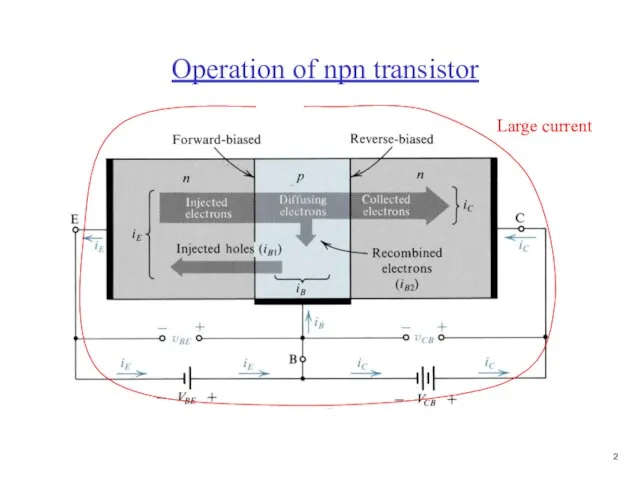
- 3. Large current Operation of npn transistor
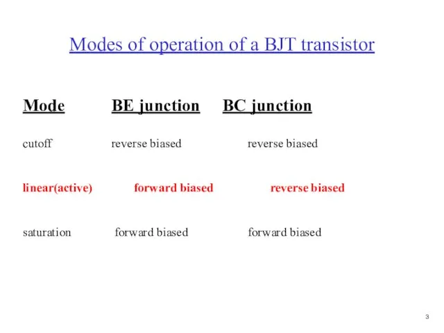
- 4. Modes of operation of a BJT transistor Mode BE junction BC junction cutoff reverse biased reverse
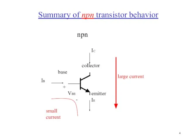
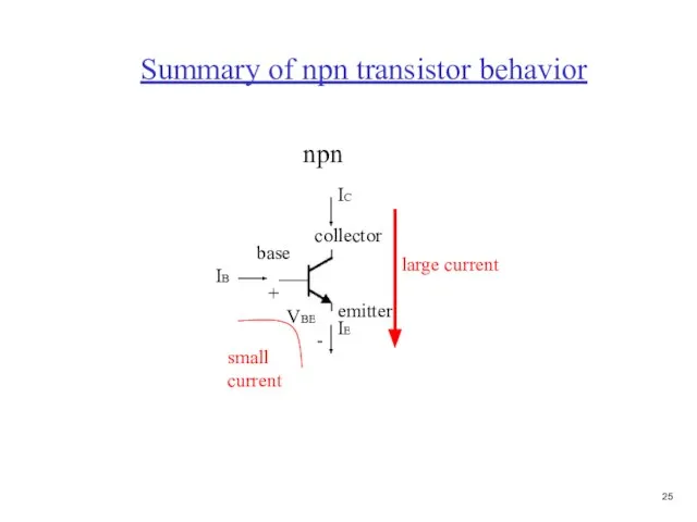
- 5. Summary of npn transistor behavior
- 6. Summary of pnp transistor behavior
- 7. Summary of equations for a BJT IE ≈ IC IC = βIB β is the current
- 8. Graphical representation of transistor characteristics IB IC IE Output circuit Input circuit
- 9. Input characteristics Acts as a diode VBE ≈0.7V IB IB VBE 0.7V
- 10. Output characteristics IC IC VCE IB = 10μA IB = 20μA IB = 30μA IB =
- 11. Biasing a transistor We must operate the transistor in the linear region. A transistor’s operating point
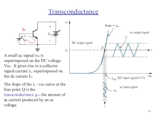
- 12. A small ac signal vbe is superimposed on the DC voltage VBE. It gives rise to
- 13. Analysis of transistor circuits at DC For all circuits: assume transistor operates in linear region write
- 14. Example-2 B-E Voltage loop 5 = IBRB + VBE, solve for IB IB = (5 -
- 15. Exercise-3 VE = 0 - .7 = -0.7V IE IC IB β = 50 IE =
- 16. Prob. Use a voltage divider, RB1 and RB2 to bias VB to avoid two power supplies.
- 17. Prob. Find the operating point Use the Thevenin equivalent circuit for the base Makes the circuit
- 18. Prob. Write B-E loop and C-E loop B-E loop C-E loop B-E loop VBB = IBRBB
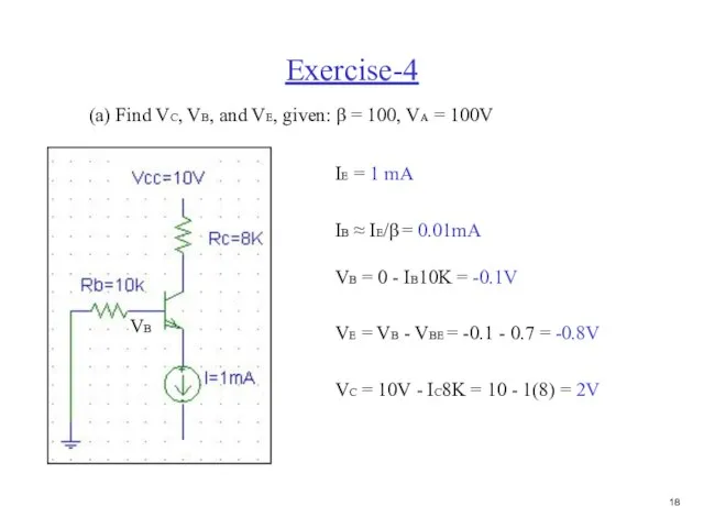
- 19. Exercise-4 (a) Find VC, VB, and VE, given: β = 100, VA = 100V IE =
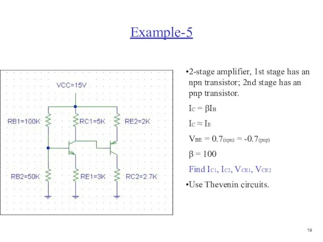
- 20. Example-5 2-stage amplifier, 1st stage has an npn transistor; 2nd stage has an pnp transistor. IC
- 21. Example -5 RBB1 = RB1||RB2 = 33K VBB1 = VCC[RB2/(RB1+RB2)] VBB1 = 15[50K/150K] = 5V Stage
- 22. Example -5 C-E loop neglect IB2 because it is IB2 IE1 IC1 VCC = IC1RC1 +
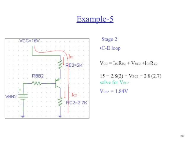
- 23. Example-5 Stage 2 B-E loop IB2 IE2 VCC = IE2RE2 + VEB +IB2RBB2 + VBB2 15
- 24. Example-5 Stage 2 C-E loop IE2 IC2 VCC = IE2RE2 + VEC2 +IC2RC2 15 = 2.8(2)
- 25. Summary of DC problem Bias transistors so that they operate in the linear region B-E junction
- 26. Summary of npn transistor behavior npn collector emitter base IB IE IC small current large current
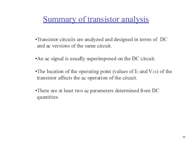
- 27. Transistor as an amplifier Transistor circuits are analyzed and designed in terms of DC and ac
- 28. A small ac signal vbe is superimposed on the DC voltage VBE. It gives rise to
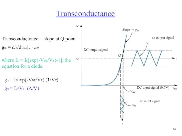
- 29. Transconductance = slope at Q point gm = dic/dvBE|ic = ICQ where IC = IS[exp(-VBE/VT)-1]; the
- 30. ac input resistance ∝ 1/slope at Q point rπ = dvBE/dib|ic = ICQ rπ ≈ VT
- 31. Small-signal equivalent circuit models ac model Hybrid-π model They are equivalent Works in linear region only
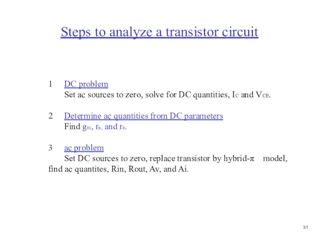
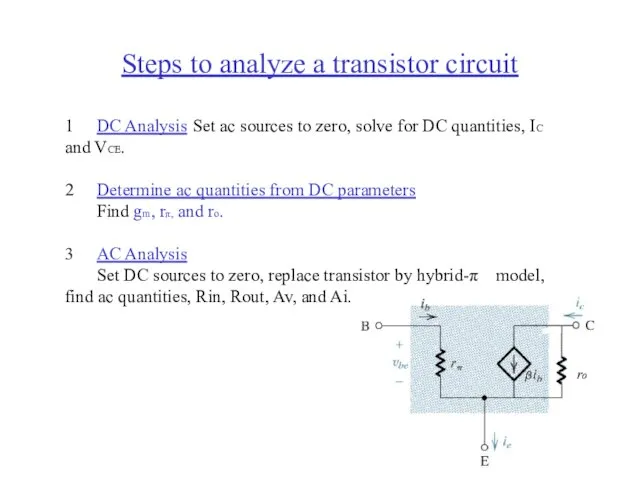
- 32. Steps to analyze a transistor circuit 1 DC problem Set ac sources to zero, solve for
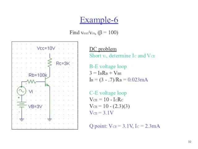
- 33. Example-6 Find vout/vin, (β = 100) DC problem Short vi, determine IC and VCE B-E voltage
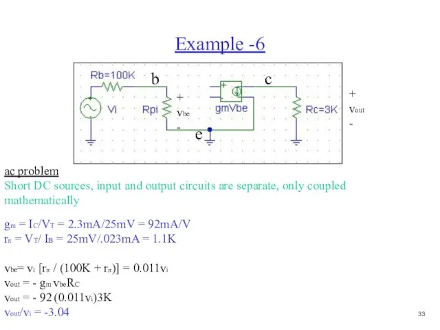
- 34. Example -6 ac problem Short DC sources, input and output circuits are separate, only coupled mathematically
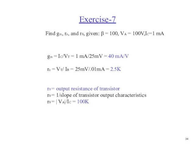
- 35. Exercise-7 Find gm, rπ, and r0, given: β = 100, VA = 100V,IC=1 mA gm =
- 36. Summary of transistor analysis Transistor circuits are analyzed and designed in terms of DC and ac
- 37. Steps to analyze a transistor circuit 1 DC Analysis Set ac sources to zero, solve for
- 38. Circuit IE = 1 mA VC = 10V - IC8K = 10 - 1(8) = 2V
- 39. ac equivalent circuit b e c vbe = (Rb||Rpi)/ [(Rb||Rpi) +Rs]vi vbe = 0.5vi vout =
- 40. Prob. + Vout - β=100
- 41. Prob. + Vout - (a) Find Rin Rin = Rpi = VT/IB = (25mV)100/.1 = 2.5KΩ
- 42. Graphical analysis Input circuit B-E voltage loop VBB = IBRB +VBE IB = (VBB - VBE)/RB
- 43. Graphical construction of IB and VBE IB = (VBB - VBE)/RB If VBE = 0, IB
- 44. Load line Output circuit C-E voltage loop VCC = ICRC +VCE IC = (VCC - VCE)/RC
- 45. Graphical construction of IC and VCE VCC/RC IC = (VCC - VCE)/RC If VCE = 0,
- 46. Graphical analysis Input signal Output signal
- 47. Load-line A results in bias point QA which is too close to VCC and thus limits
- 48. Basic single-stage BJT amplifier configurations We will study 3 types of BJT amplifiers CE - common
- 49. Common emitter amplifier ac equivalent circuit
- 50. Common emitter amplifier Rin Rout + Vout - Rin (Does not include source) Rin = Rpi
- 51. Common emitter with RE amplifier ac equivalent circuit
- 52. Common emitter with RE amplifier Rin Rout + Vout - Rin Rin = V/ib V =
- 53. Common collector (emitter follower) amplifier b c e + vout - (vout at emitter) ac equivalent
- 54. Common collector amplifier Rin + vout - Rin Rin = V/ib V = ib Rpi +
- 55. Common collector amplifier Rout + vout - Rout (don’t include RL, set Vs = 0) Rout
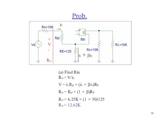
- 56. Prob ac circuit CE with RE amp, because RE is in ac circuit Given Rpi =VT/IB
- 57. Prob. (a) Find Rin Rin = V/ib V = ib Rpi + (ib + βib)RE Rin
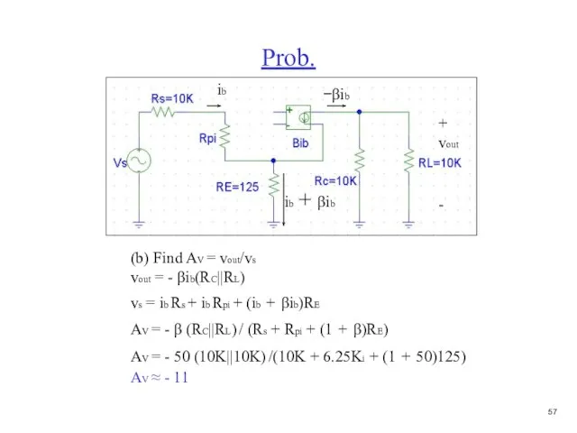
- 58. Prob. (b) Find AV = vout/vs vout = - βib(RC||RL) vs = ib Rs + ib
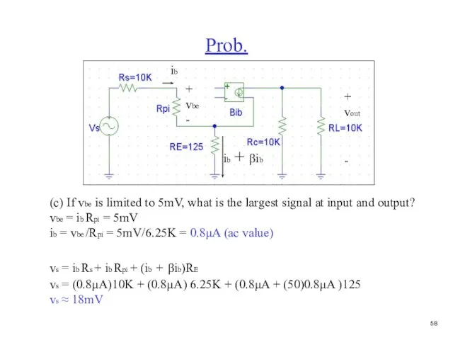
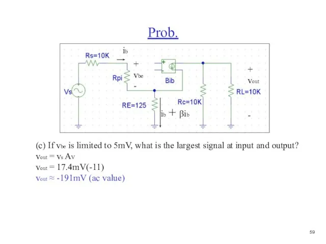
- 59. Prob. (c) If vbe is limited to 5mV, what is the largest signal at input and
- 60. Prob. (c) If vbe is limited to 5mV, what is the largest signal at input and
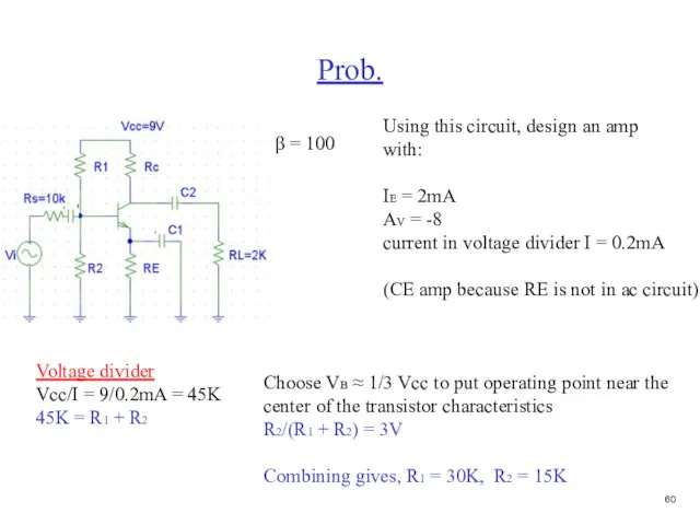
- 61. Prob. Using this circuit, design an amp with: IE = 2mA AV = -8 current in
- 62. Prob. β = 100 Find RE (input circuit) Use Thevenin equivalent B-E loop VBB=IBRBB+VBE+IERE using IB
- 63. Prob. Find Rc (ac circuit) Rpi = VT/IB = 25mV(100)/2mA = 1.25K Ro = VA/IC =
- 64. CE amplifier
- 65. CE amplifier Av ≈ -12.2
- 66. FOURIER COMPONENTS OF TRANSIENT RESPONSE V($N_0009) DC COMPONENT = -1.226074E-01 HARMONIC FREQUENCY FOURIER NORMALIZED PHASE NORMALIZED
- 67. CE amplifier with RE
- 68. CE amplifier with RE Av ≈ - 7.5
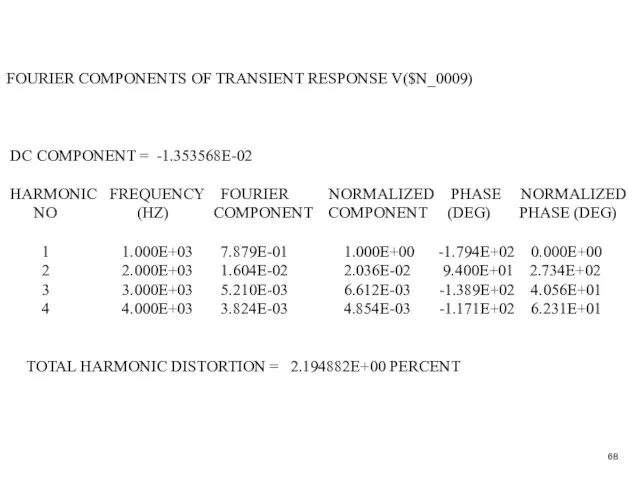
- 69. FOURIER COMPONENTS OF TRANSIENT RESPONSE V($N_0009) DC COMPONENT = -1.353568E-02 HARMONIC FREQUENCY FOURIER NORMALIZED PHASE NORMALIZED
- 70. Summary Av THD CE -12.2 12.7% CE w/RE (RE = 100) -7.5 2.19%
- 71. Prob. + vout - 2 stage amplifier (a) Find IC and VC of each transistor Both
- 72. Prob. (a) Find IC and VC of each transistor (same for each stage) B-E voltage loop
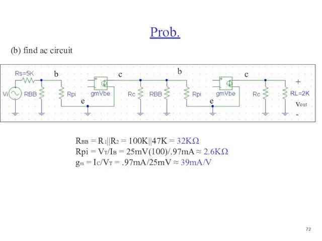
- 73. Prob. b c e + vout - (b) find ac circuit b c e RBB =
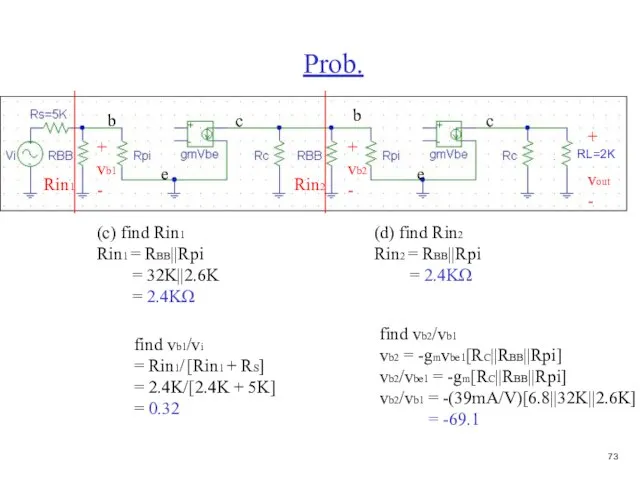
- 74. Prob. b c e + vout - (c) find Rin1 Rin1 = RBB||Rpi = 32K||2.6K =
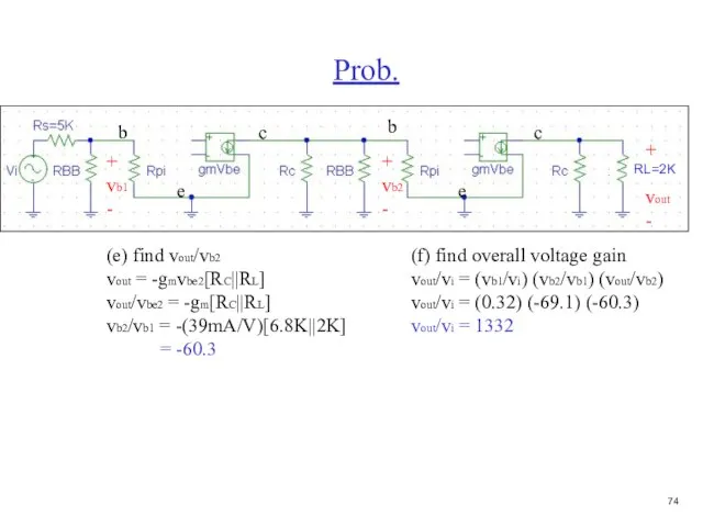
- 75. Prob. b c e + vout - (e) find vout/vb2 vout = -gmvbe2[RC||RL] vout/vbe2 = -gm[RC||RL]
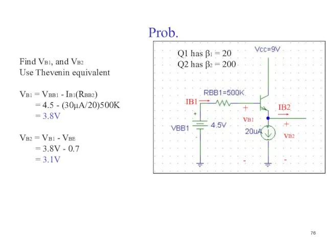
- 76. Prob. Find IE1, IE2, VB1, and VB2 IE2 = 2mA IE1 = I20μA + IB2 IE1
- 77. Prob. Find VB1, and VB2 Use Thevenin equivalent VB1 = VBB1 - IB1(RBB2) = 4.5 -
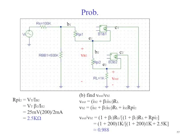
- 78. Prob. (b) find vout/vb2 vout = (ib2 + β2ib2)RL vb2 = (ib2 + β2ib2)RL + ib2Rpi2
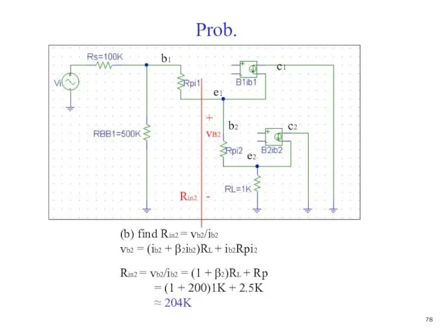
- 79. Prob. (b) find Rin2 = vb2/ib2 vb2 = (ib2 + β2ib2)RL + ib2Rpi2 Rin2 = vb2/ib2
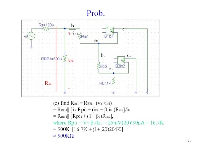
- 80. Prob. (c) find Rin1 = RBB1||(vb1/ib1) = RBB1|| [ib1Rpi1 + (ib1 + β1ib1)Rin2]/ib1 = RBB1|| [Rpi1
- 81. Prob. (c) find ve1/vb1 ve1 = (ib1 + β1ib1)Rin2 vb1 = (ib1 + β1ib1)Rin2 + ib1Rpi1
- 82. Prob. (d) find vb1/vi vb1/vi = Rin1/[RS + Rin1] = 0.82 b1 e1 c1 b2 e2
- 83. Voltage outputs at each stage Output of stage 2 Output of stage 1 Input
- 84. Current Input current Input to stage 2 (ib2)
- 85. Current output current Input to stage 2 (ib2)
- 86. Current output current Input to stage 2 (ib2) Input current
- 87. Power and current gain Input current = (Vi)/Rin = 1/500K = 2.0μA output current= (Vout)/RL =
- 88. BJT Output Characteristics Plot Ic vs. Vce for multiple values of Vce and Ib From Analysis
- 89. Probe: BJT Output Characteristics 1 Result of probe 2 Add plot (plot menu) -> Add trace
- 90. BJT Output Characteristics: current gain Ib = 5μA (Each plot 10μA difference) β at Vce =
- 91. BJT Output Characteristics: transistor output resistance Ib = 5μA (Each plot 10μA difference) Ro = 1/slope
- 92. CE Amplifier: Measurements with Spice Rin Rout
- 93. Input Resistance Measurement Using SPICE Replace source, Vs and Rs with Vin, measure Rin = Vin/Iin
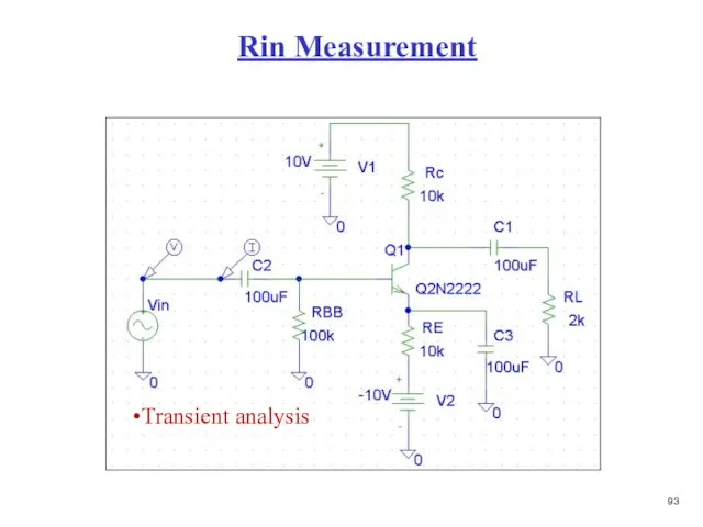
- 94. Rin Measurement Transient analysis
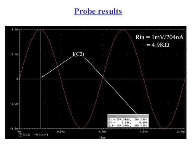
- 95. Probe results I(C2) Rin = 1mV/204nA = 4.9KΩ
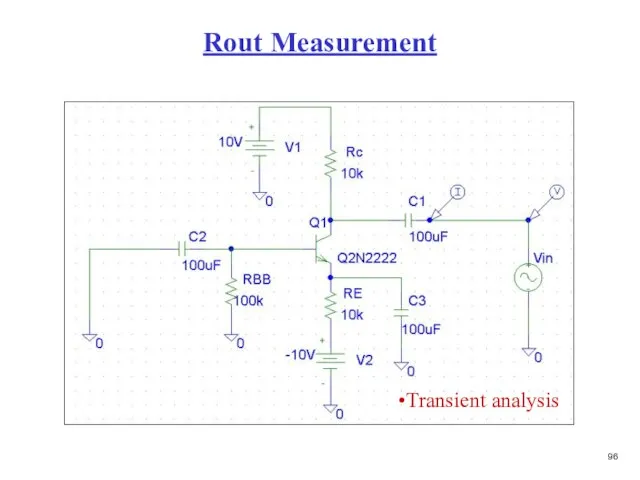
- 96. Output Resistance Measurement Using SPICE Replace load, RL with Vin, measure Rin = Vin/Iin Set Vs
- 97. Rout Measurement Transient analysis
- 98. Probe results -I(C1) Rout = 1mV/111nA = 9KΩ -I(C1) is current in Vin flowing out of
- 99. DC Power measurements Power delivered by + 10 sources: (10)(872μA) + (10)(877μA) = 8.72mW + 8.77mW
- 101. Скачать презентацию
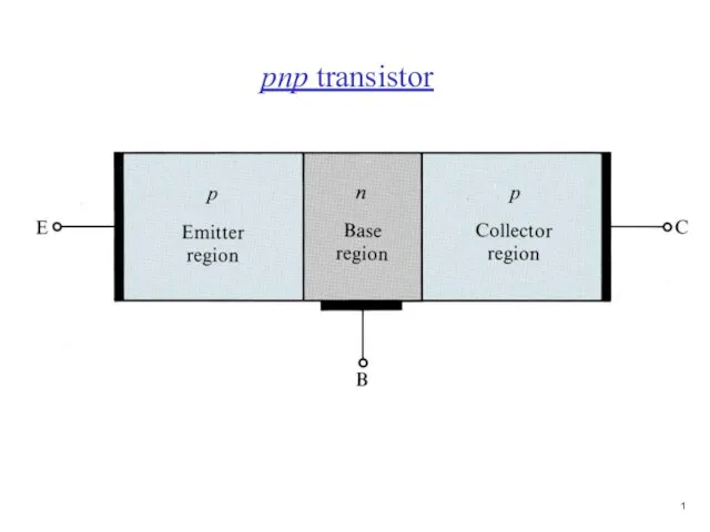
Слайд 3Large current
Operation of npn transistor
Large current
Operation of npn transistor
Слайд 4Modes of operation of a BJT transistor
Mode BE junction BC junction
cutoff reverse biased reverse biased
linear(active) forward
Modes of operation of a BJT transistor
Mode BE junction BC junction
cutoff reverse biased reverse biased
linear(active) forward
Слайд 5Summary of npn transistor behavior
Summary of npn transistor behavior
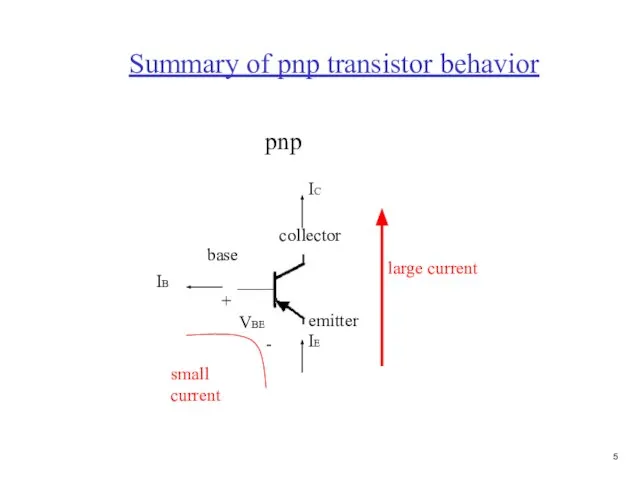
Слайд 6Summary of pnp transistor behavior
Summary of pnp transistor behavior
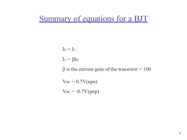
Слайд 7Summary of equations for a BJT
IE ≈ IC
IC = βIB
β is the
Summary of equations for a BJT
IE ≈ IC
IC = βIB
β is the
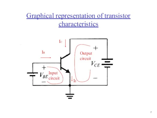
Слайд 8Graphical representation of transistor characteristics
IB
IC
IE
Output
circuit
Input
circuit
Graphical representation of transistor characteristics
IB
IC
IE
Output
circuit
Input
circuit
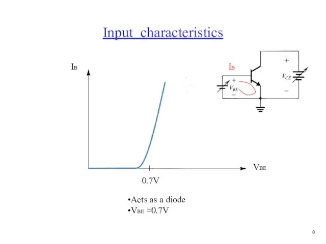
Слайд 9Input characteristics
Acts as a diode
VBE ≈0.7V
IB
IB
VBE
0.7V
Input characteristics
Acts as a diode
VBE ≈0.7V
IB
IB
VBE
0.7V
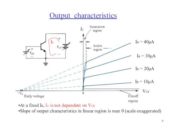
Слайд 10Output characteristics
IC
IC
VCE
IB = 10μA
IB = 20μA
IB = 30μA
IB = 40μA
Cutoff
region
At a fixed
Output characteristics
IC
IC
VCE
IB = 10μA
IB = 20μA
IB = 30μA
IB = 40μA
Cutoff
region
At a fixed
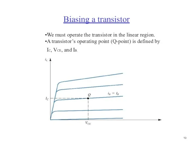
Слайд 11Biasing a transistor
We must operate the transistor in the linear region.
A transistor’s
Biasing a transistor
We must operate the transistor in the linear region.
A transistor’s
Слайд 12A small ac signal vbe is superimposed on the DC voltage VBE.
A small ac signal vbe is superimposed on the DC voltage VBE.

Слайд 13Analysis of transistor circuits at DC
For all circuits: assume transistor operates in
Analysis of transistor circuits at DC
For all circuits: assume transistor operates in
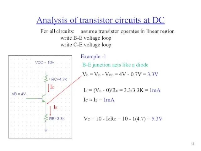
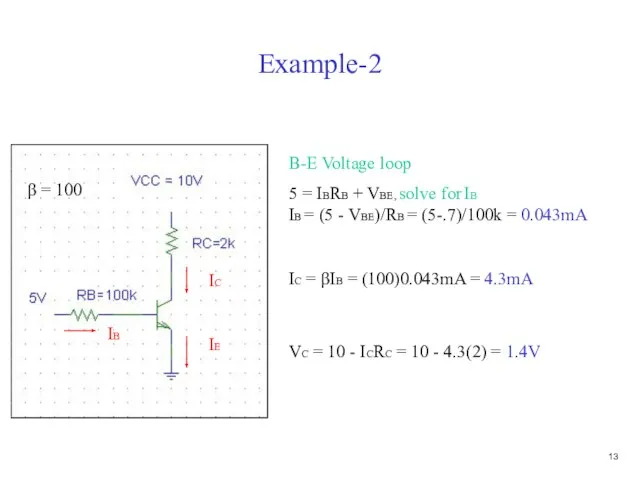
Слайд 14Example-2
B-E Voltage loop
5 = IBRB + VBE, solve for IB
IB = (5
Example-2
B-E Voltage loop
5 = IBRB + VBE, solve for IB
IB = (5
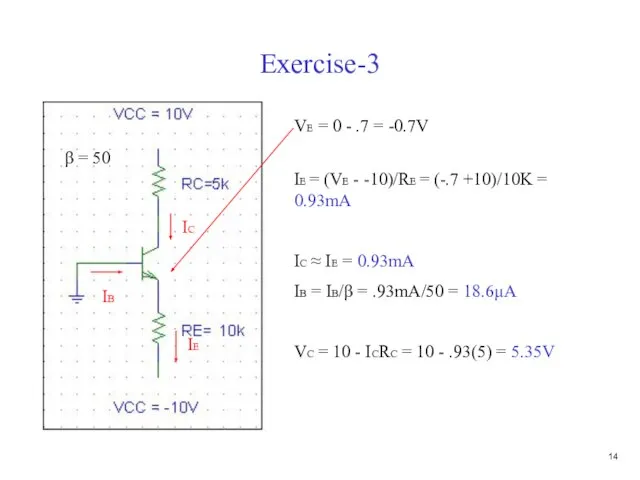
Слайд 15Exercise-3
VE = 0 - .7 = -0.7V
IE
IC
IB
β = 50
IE = (VE -
Exercise-3
VE = 0 - .7 = -0.7V
IE
IC
IB
β = 50
IE = (VE -
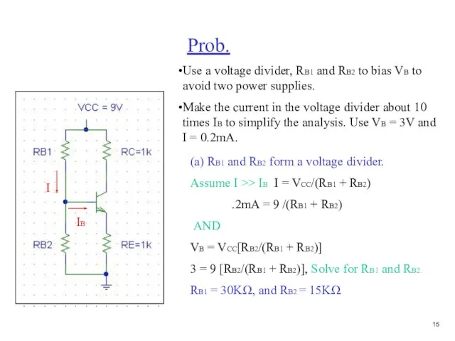
Слайд 16Prob.
Use a voltage divider, RB1 and RB2 to bias VB to
Prob.
Use a voltage divider, RB1 and RB2 to bias VB to
Слайд 17Prob.
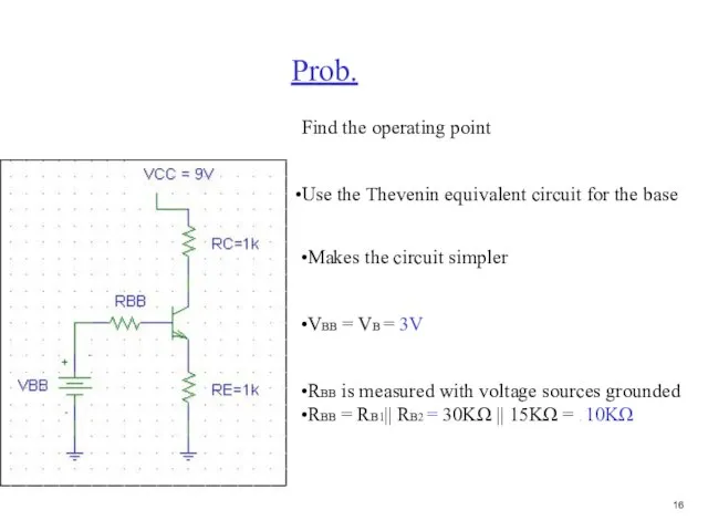
Find the operating point
Use the Thevenin equivalent circuit for the base
Makes the
Prob.
Find the operating point
Use the Thevenin equivalent circuit for the base
Makes the
Слайд 18Prob.
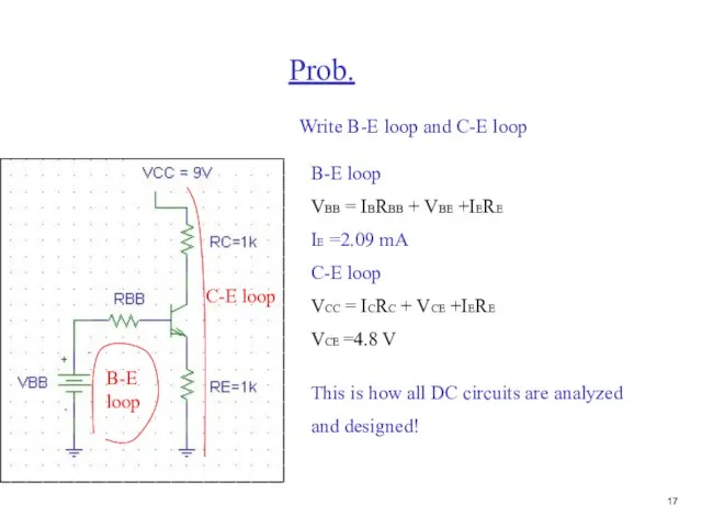
Write B-E loop and C-E loop
B-E
loop
C-E loop
B-E loop
VBB = IBRBB + VBE
Prob.
Write B-E loop and C-E loop
B-E
loop
C-E loop
B-E loop
VBB = IBRBB + VBE
Слайд 19Exercise-4
(a) Find VC, VB, and VE, given: β = 100, VA =
Exercise-4
(a) Find VC, VB, and VE, given: β = 100, VA =
Слайд 20Example-5
2-stage amplifier, 1st stage has an npn transistor; 2nd stage has an
Example-5
2-stage amplifier, 1st stage has an npn transistor; 2nd stage has an
Слайд 21Example -5
RBB1 = RB1||RB2 = 33K
VBB1 = VCC[RB2/(RB1+RB2)]
VBB1 = 15[50K/150K] =
Example -5
RBB1 = RB1||RB2 = 33K
VBB1 = VCC[RB2/(RB1+RB2)]
VBB1 = 15[50K/150K] =
![Example -5 RBB1 = RB1||RB2 = 33K VBB1 = VCC[RB2/(RB1+RB2)] VBB1 =](/_ipx/f_webp&q_80&fit_contain&s_1440x1080/imagesDir/jpg/374487/slide-20.jpg)
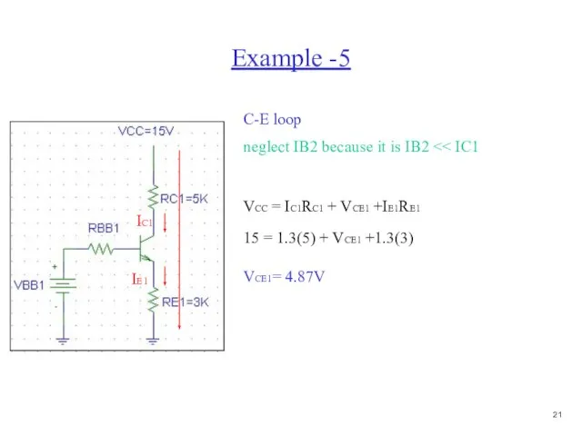
Слайд 22Example -5
C-E loop
neglect IB2 because it is IB2 << IC1
IE1
IC1
VCC = IC1RC1
Example -5
C-E loop
neglect IB2 because it is IB2 << IC1
IE1
IC1
VCC = IC1RC1
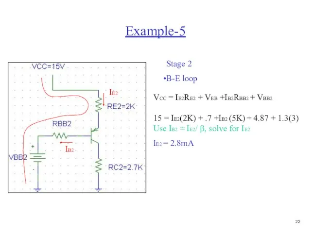
Слайд 23Example-5
Stage 2
B-E loop
IB2
IE2
VCC = IE2RE2 + VEB +IB2RBB2 + VBB2
15 = IE2(2K)
Example-5
Stage 2
B-E loop
IB2
IE2
VCC = IE2RE2 + VEB +IB2RBB2 + VBB2
15 = IE2(2K)
Слайд 24Example-5
Stage 2
C-E loop
IE2
IC2
VCC = IE2RE2 + VEC2 +IC2RC2
15 = 2.8(2) + VEC2
Example-5
Stage 2
C-E loop
IE2
IC2
VCC = IE2RE2 + VEC2 +IC2RC2
15 = 2.8(2) + VEC2
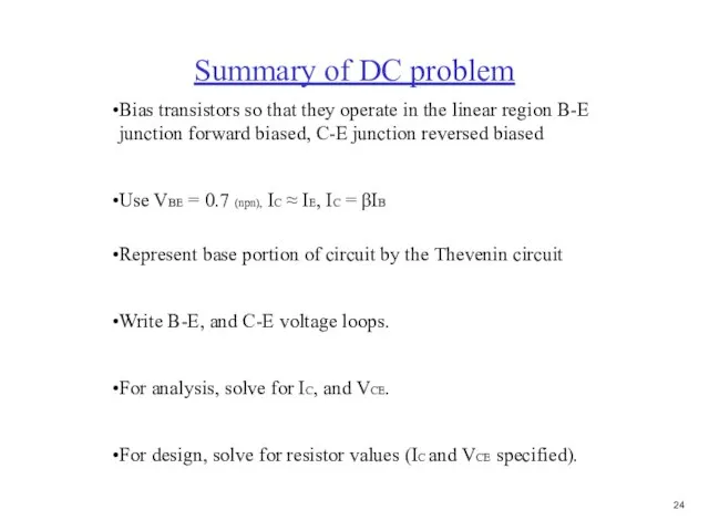
Слайд 25Summary of DC problem
Bias transistors so that they operate in the linear
Summary of DC problem
Bias transistors so that they operate in the linear
Слайд 26Summary of npn transistor behavior
npn
collector
emitter
base
IB
IE
IC
small
current
large current
+
VBE
-
Summary of npn transistor behavior
npn
collector
emitter
base
IB
IE
IC
small
current
large current
+
VBE
-
Слайд 27 Transistor as an amplifier
Transistor circuits are analyzed and designed in terms
Transistor as an amplifier
Transistor circuits are analyzed and designed in terms
Слайд 28A small ac signal vbe is superimposed on the DC voltage VBE.
A small ac signal vbe is superimposed on the DC voltage VBE.
Слайд 29Transconductance = slope at Q point
gm = dic/dvBE|ic = ICQ
where IC =
Transconductance = slope at Q point
gm = dic/dvBE|ic = ICQ
where IC =
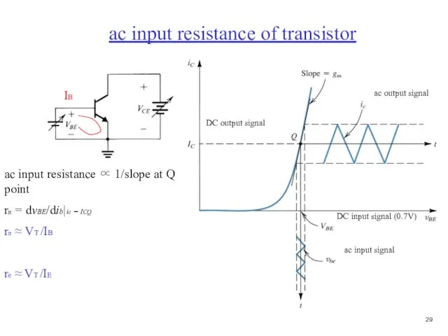
Слайд 30ac input resistance ∝ 1/slope at Q point
rπ = dvBE/dib|ic = ICQ
rπ
ac input resistance ∝ 1/slope at Q point
rπ = dvBE/dib|ic = ICQ
rπ
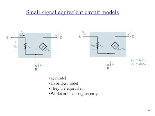
Слайд 31Small-signal equivalent circuit models
ac model
Hybrid-π model
They are equivalent
Works in linear region only
Small-signal equivalent circuit models
ac model
Hybrid-π model
They are equivalent
Works in linear region only
Слайд 32Steps to analyze a transistor circuit
1 DC problem
Set ac sources to zero, solve
Steps to analyze a transistor circuit
1 DC problem
Set ac sources to zero, solve
Слайд 33Example-6
Find vout/vin, (β = 100)
DC problem
Short vi, determine IC and VCE
B-E voltage
Example-6
Find vout/vin, (β = 100)
DC problem
Short vi, determine IC and VCE
B-E voltage
Слайд 34Example -6
ac problem
Short DC sources, input and output circuits are separate, only
Example -6
ac problem
Short DC sources, input and output circuits are separate, only
Слайд 35Exercise-7
Find gm, rπ, and r0, given: β = 100, VA =
Exercise-7
Find gm, rπ, and r0, given: β = 100, VA =
Слайд 36Summary of transistor analysis
Transistor circuits are analyzed and designed in terms of
Summary of transistor analysis
Transistor circuits are analyzed and designed in terms of
Слайд 37Steps to analyze a transistor circuit
1 DC Analysis Set ac sources to zero, solve
Steps to analyze a transistor circuit
1 DC Analysis Set ac sources to zero, solve
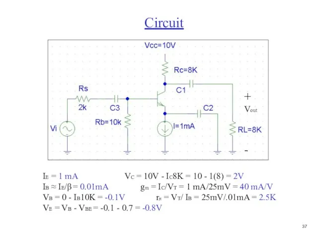
Слайд 38Circuit
IE = 1 mA VC = 10V - IC8K = 10 -
Circuit
IE = 1 mA VC = 10V - IC8K = 10 -
Слайд 39ac equivalent circuit
b
e
c
vbe = (Rb||Rpi)/ [(Rb||Rpi) +Rs]vi
vbe = 0.5vi
vout = -(gmvbe)||(Ro||Rc ||RL)
vout
ac equivalent circuit
b
e
c
vbe = (Rb||Rpi)/ [(Rb||Rpi) +Rs]vi
vbe = 0.5vi
vout = -(gmvbe)||(Ro||Rc ||RL)
vout
![ac equivalent circuit b e c vbe = (Rb||Rpi)/ [(Rb||Rpi) +Rs]vi vbe](/_ipx/f_webp&q_80&fit_contain&s_1440x1080/imagesDir/jpg/374487/slide-38.jpg)
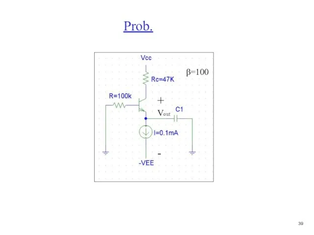
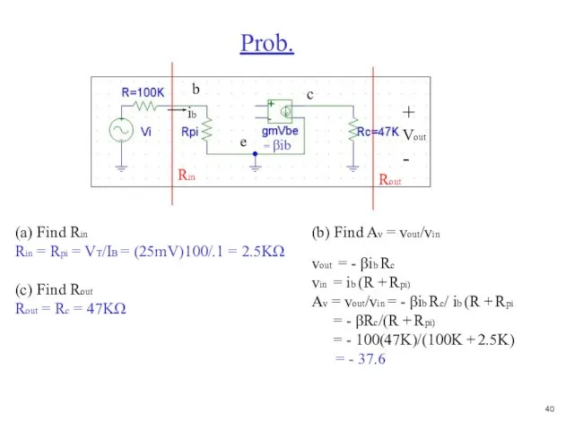
Слайд 40Prob.
+
Vout
-
β=100
Prob.
+
Vout
-
β=100
Слайд 41Prob.
+
Vout
-
(a) Find Rin
Rin = Rpi = VT/IB = (25mV)100/.1 = 2.5KΩ
(c)
Prob.
+
Vout
-
(a) Find Rin
Rin = Rpi = VT/IB = (25mV)100/.1 = 2.5KΩ
(c)
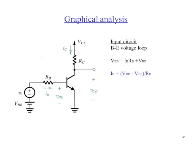
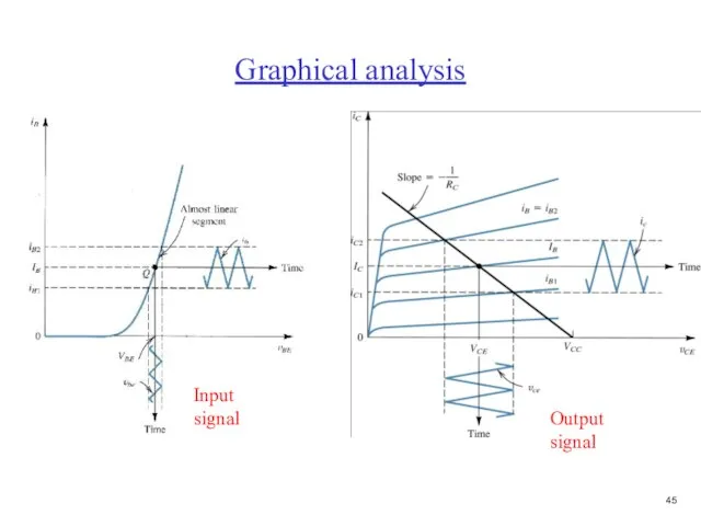
Слайд 42Graphical analysis
Input circuit
B-E voltage loop
VBB = IBRB +VBE
IB = (VBB - VBE)/RB
Graphical analysis
Input circuit
B-E voltage loop
VBB = IBRB +VBE
IB = (VBB - VBE)/RB
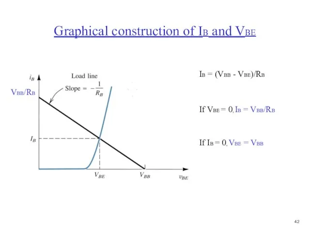
Слайд 43Graphical construction of IB and VBE
IB = (VBB - VBE)/RB
If VBE =
Graphical construction of IB and VBE
IB = (VBB - VBE)/RB
If VBE =
Слайд 44Load line
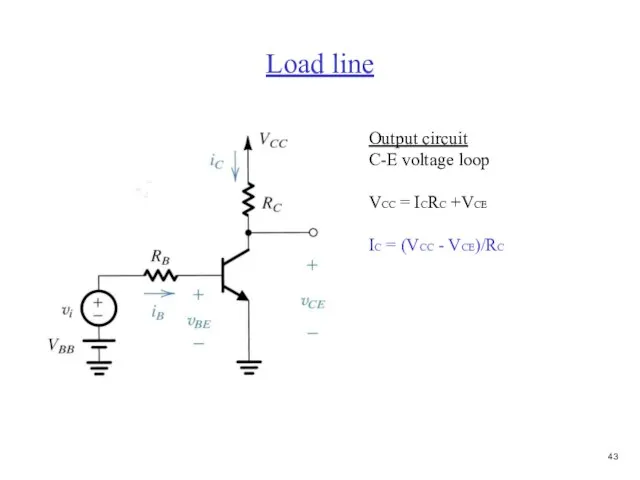
Output circuit
C-E voltage loop
VCC = ICRC +VCE
IC = (VCC - VCE)/RC
Load line
Output circuit
C-E voltage loop
VCC = ICRC +VCE
IC = (VCC - VCE)/RC
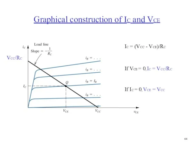
Слайд 45Graphical construction of IC and VCE
VCC/RC
IC = (VCC - VCE)/RC
If VCE =
Graphical construction of IC and VCE
VCC/RC
IC = (VCC - VCE)/RC
If VCE =
Слайд 46Graphical analysis
Input
signal
Output
signal
Graphical analysis
Input
signal
Output
signal
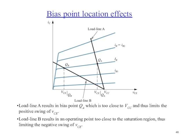
Слайд 47Load-line A results in bias point QA which is too close to
Load-line A results in bias point QA which is too close to
Слайд 48Basic single-stage BJT amplifier configurations
We will study 3 types of BJT
Basic single-stage BJT amplifier configurations
We will study 3 types of BJT
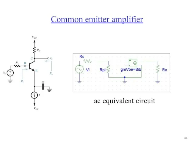
Слайд 49Common emitter amplifier
ac equivalent circuit
Common emitter amplifier
ac equivalent circuit
Слайд 50Common emitter amplifier
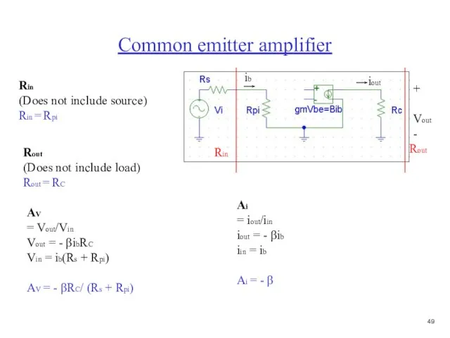
Rin
Rout
+
Vout
-
Rin
(Does not include source)
Rin = Rpi
Rout
(Does not include load)
Rout =
Common emitter amplifier
Rin
Rout
+
Vout
-
Rin
(Does not include source)
Rin = Rpi
Rout
(Does not include load)
Rout =
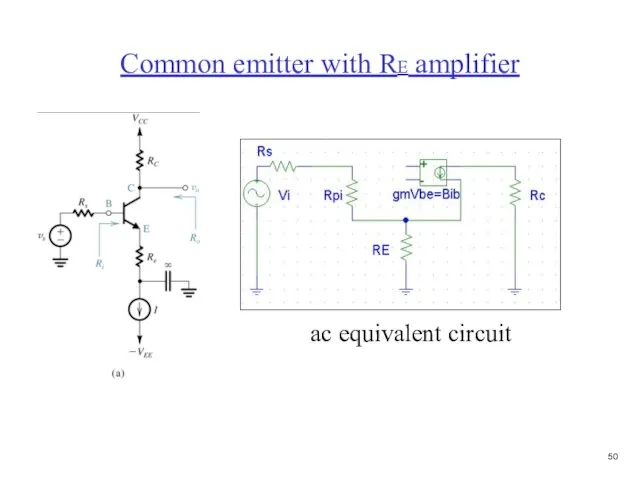
Слайд 51Common emitter with RE amplifier
ac equivalent circuit
Common emitter with RE amplifier
ac equivalent circuit
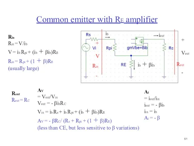
Слайд 52Common emitter with RE amplifier
Rin
Rout
+
Vout
-
Rin
Rin = V/ib
V = ib Rpi + (ib
Common emitter with RE amplifier
Rin
Rout
+
Vout
-
Rin
Rin = V/ib
V = ib Rpi + (ib
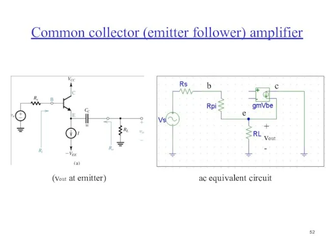
Слайд 53Common collector (emitter follower) amplifier
b
c
e
+
vout
-
(vout at emitter)
ac equivalent circuit
Common collector (emitter follower) amplifier
b
c
e
+
vout
-
(vout at emitter)
ac equivalent circuit
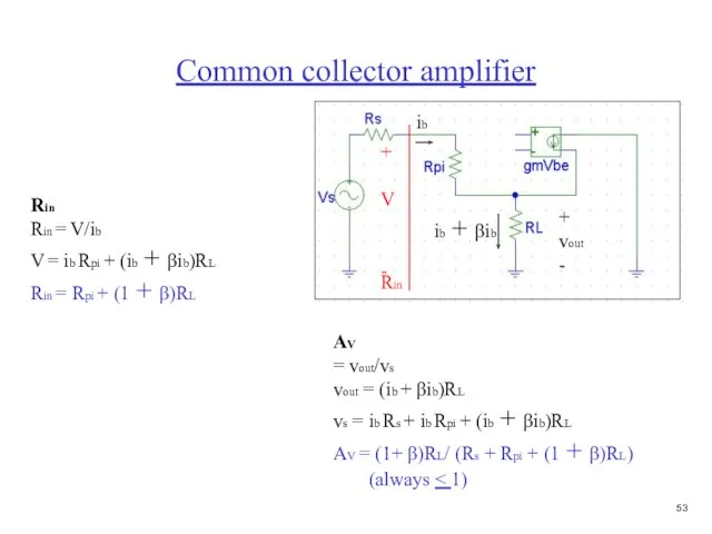
Слайд 54Common collector amplifier
Rin
+
vout
-
Rin
Rin = V/ib
V = ib Rpi + (ib + βib)RL
Rin
Common collector amplifier
Rin
+
vout
-
Rin
Rin = V/ib
V = ib Rpi + (ib + βib)RL
Rin
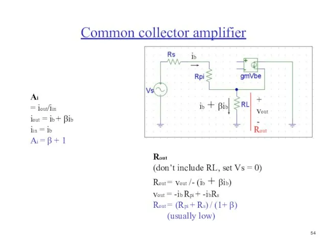
Слайд 55Common collector amplifier
Rout
+
vout
-
Rout
(don’t include RL, set Vs = 0)
Rout = vout
Common collector amplifier
Rout
+
vout
-
Rout
(don’t include RL, set Vs = 0)
Rout = vout
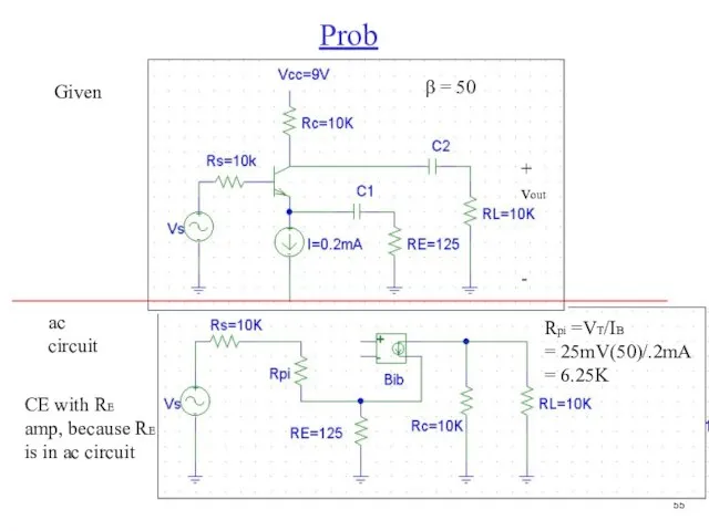
Слайд 56Prob
ac
circuit
CE with RE
amp, because RE
is in ac circuit
Given
Rpi =VT/IB
= 25mV(50)/.2mA
= 6.25K
Prob
ac
circuit
CE with RE
amp, because RE
is in ac circuit
Given
Rpi =VT/IB
= 25mV(50)/.2mA
= 6.25K
Слайд 57Prob.
(a) Find Rin
Rin = V/ib
V = ib Rpi + (ib +
Prob.
(a) Find Rin
Rin = V/ib
V = ib Rpi + (ib +
Слайд 58Prob.
(b) Find AV = vout/vs
vout = - βib(RC||RL)
vs = ib Rs
Prob.
(b) Find AV = vout/vs
vout = - βib(RC||RL)
vs = ib Rs
Слайд 59Prob.
(c) If vbe is limited to 5mV, what is the largest
Prob.
(c) If vbe is limited to 5mV, what is the largest
Слайд 60Prob.
(c) If vbe is limited to 5mV, what is the largest
Prob.
(c) If vbe is limited to 5mV, what is the largest
Слайд 61Prob.
Using this circuit, design an amp
with:
IE = 2mA
AV = -8
current in voltage
Prob.
Using this circuit, design an amp
with:
IE = 2mA
AV = -8
current in voltage
Слайд 62Prob.
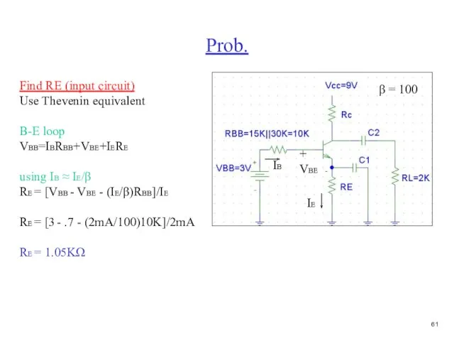
β = 100
Find RE (input circuit)
Use Thevenin equivalent
B-E loop
VBB=IBRBB+VBE+IERE
using IB ≈ IE/β
RE
Prob.
β = 100
Find RE (input circuit)
Use Thevenin equivalent
B-E loop
VBB=IBRBB+VBE+IERE
using IB ≈ IE/β
RE
Слайд 63Prob.
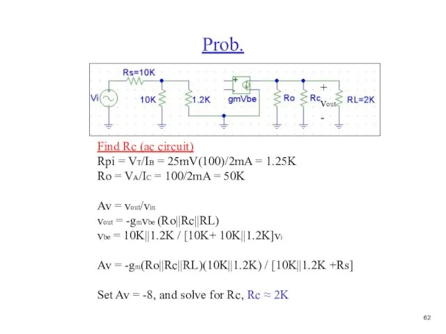
Find Rc (ac circuit)
Rpi = VT/IB = 25mV(100)/2mA = 1.25K
Ro = VA/IC
Prob.
Find Rc (ac circuit)
Rpi = VT/IB = 25mV(100)/2mA = 1.25K
Ro = VA/IC
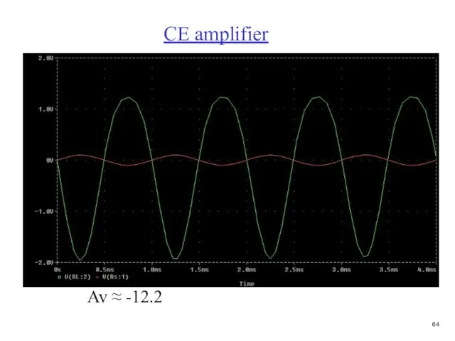
Слайд 64CE amplifier
CE amplifier
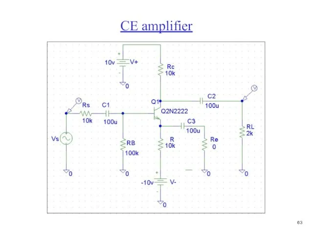
Слайд 65CE amplifier
Av ≈ -12.2
CE amplifier
Av ≈ -12.2
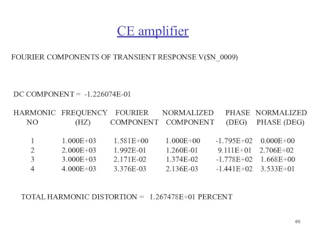
Слайд 66FOURIER COMPONENTS OF TRANSIENT RESPONSE V($N_0009)
DC COMPONENT = -1.226074E-01
HARMONIC FREQUENCY FOURIER
DC COMPONENT = -1.226074E-01
HARMONIC FREQUENCY FOURIER
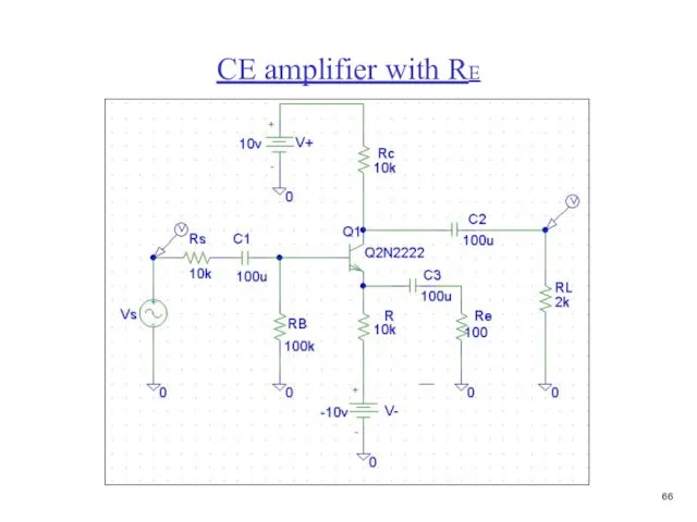
Слайд 67CE amplifier with RE
CE amplifier with RE
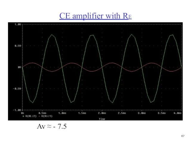
Слайд 68CE amplifier with RE
Av ≈ - 7.5
CE amplifier with RE
Av ≈ - 7.5
Слайд 69FOURIER COMPONENTS OF TRANSIENT RESPONSE V($N_0009)
DC COMPONENT = -1.353568E-02
HARMONIC FREQUENCY FOURIER
FOURIER COMPONENTS OF TRANSIENT RESPONSE V($N_0009)
DC COMPONENT = -1.353568E-02
HARMONIC FREQUENCY FOURIER
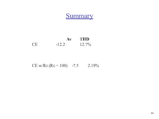
Слайд 70Summary
Av THD
CE -12.2 12.7%
CE w/RE (RE = 100) -7.5 2.19%
Summary
Av THD
CE -12.2 12.7%
CE w/RE (RE = 100) -7.5 2.19%
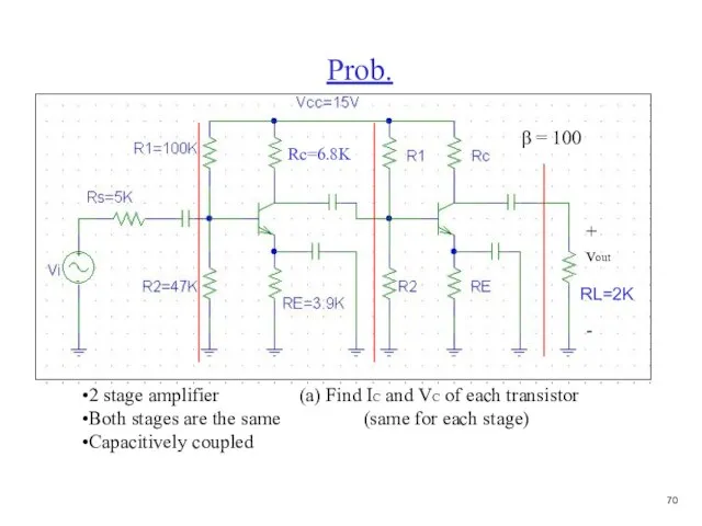
Слайд 71Prob.
+
vout
-
2 stage amplifier (a) Find IC and VC of each transistor
Both stages are
Prob.
+
vout
-
2 stage amplifier (a) Find IC and VC of each transistor
Both stages are
Слайд 72Prob.
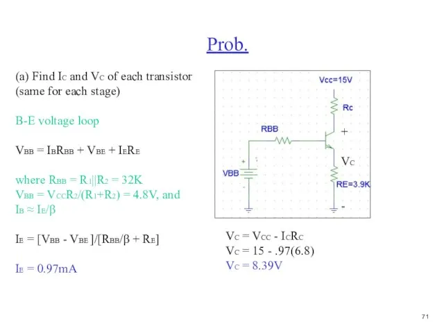
(a) Find IC and VC of each transistor
(same for each stage)
B-E
Prob.
(a) Find IC and VC of each transistor
(same for each stage)
B-E
Слайд 73Prob.
b
c
e
+
vout
-
(b) find ac circuit
b
c
e
RBB = R1||R2 = 100K||47K = 32KΩ
Rpi
Prob.
b
c
e
+
vout
-
(b) find ac circuit
b
c
e
RBB = R1||R2 = 100K||47K = 32KΩ
Rpi
Слайд 74Prob.
b
c
e
+
vout
-
(c) find Rin1
Rin1 = RBB||Rpi
= 32K||2.6K
= 2.4KΩ
b
c
e
Rin1
(d) find Rin2
Rin2
Prob.
b
c
e
+
vout
-
(c) find Rin1
Rin1 = RBB||Rpi
= 32K||2.6K
= 2.4KΩ
b
c
e
Rin1
(d) find Rin2
Rin2
Слайд 75Prob.
b
c
e
+
vout
-
(e) find vout/vb2
vout = -gmvbe2[RC||RL]
vout/vbe2 = -gm[RC||RL]
vb2/vb1 = -(39mA/V)[6.8K||2K]
= -60.3
b
c
e
(f)
Prob.
b
c
e
+
vout
-
(e) find vout/vb2
vout = -gmvbe2[RC||RL]
vout/vbe2 = -gm[RC||RL]
vb2/vb1 = -(39mA/V)[6.8K||2K]
= -60.3
b
c
e
(f)
Слайд 76Prob.
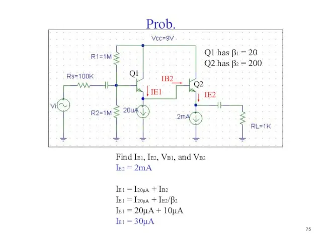
Find IE1, IE2, VB1, and VB2
IE2 = 2mA
IE1 = I20μA +
Prob.
Find IE1, IE2, VB1, and VB2
IE2 = 2mA
IE1 = I20μA +
Слайд 77Prob.
Find VB1, and VB2
Use Thevenin equivalent
VB1 = VBB1 - IB1(RBB2)
=
Prob.
Find VB1, and VB2
Use Thevenin equivalent
VB1 = VBB1 - IB1(RBB2)
=
Слайд 78Prob.
(b) find vout/vb2
vout = (ib2 + β2ib2)RL
vb2 = (ib2 + β2ib2)RL
Prob.
(b) find vout/vb2
vout = (ib2 + β2ib2)RL
vb2 = (ib2 + β2ib2)RL
Слайд 79Prob.
(b) find Rin2 = vb2/ib2
vb2 = (ib2 + β2ib2)RL + ib2Rpi2
Rin2
Prob.
(b) find Rin2 = vb2/ib2
vb2 = (ib2 + β2ib2)RL + ib2Rpi2
Rin2
Слайд 80Prob.
(c) find Rin1 = RBB1||(vb1/ib1)
= RBB1|| [ib1Rpi1 + (ib1 + β1ib1)Rin2]/ib1
= RBB1||
Prob.
(c) find Rin1 = RBB1||(vb1/ib1)
= RBB1|| [ib1Rpi1 + (ib1 + β1ib1)Rin2]/ib1
= RBB1||
Слайд 81Prob.
(c) find ve1/vb1
ve1 = (ib1 + β1ib1)Rin2
vb1 = (ib1 + β1ib1)Rin2
Prob.
(c) find ve1/vb1
ve1 = (ib1 + β1ib1)Rin2
vb1 = (ib1 + β1ib1)Rin2
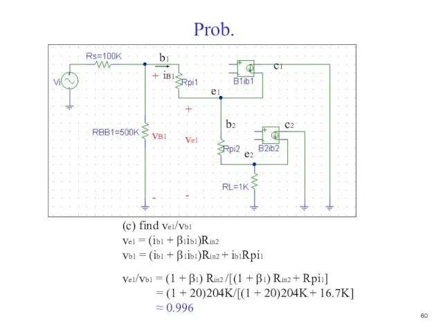
Слайд 82Prob.
(d) find vb1/vi
vb1/vi = Rin1/[RS + Rin1]
= 0.82
b1
e1
c1
b2
e2
c2
+
vb1
-
(e) find overall
Prob.
(d) find vb1/vi
vb1/vi = Rin1/[RS + Rin1]
= 0.82
b1
e1
c1
b2
e2
c2
+
vb1
-
(e) find overall
![Prob. (d) find vb1/vi vb1/vi = Rin1/[RS + Rin1] = 0.82 b1](/_ipx/f_webp&q_80&fit_contain&s_1440x1080/imagesDir/jpg/374487/slide-81.jpg)
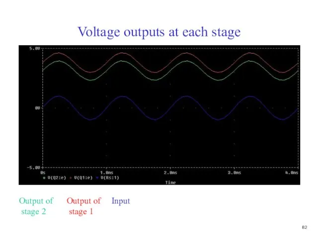
Слайд 83Voltage outputs at each stage
Output of
stage 2
Output of
stage 1
Input
Voltage outputs at each stage
Output of
stage 2
Output of
stage 1
Input
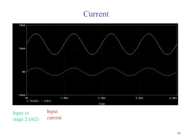
Слайд 84 Current
Input
current
Input to
stage 2 (ib2)
Current
Input
current
Input to
stage 2 (ib2)
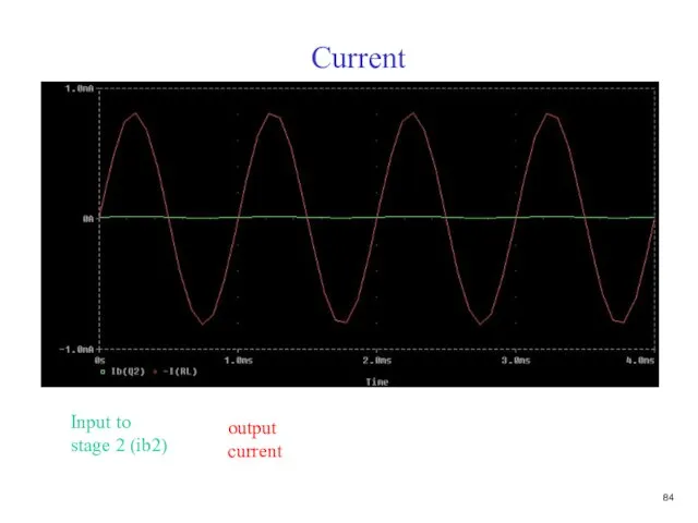
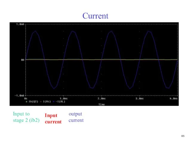
Слайд 85 Current
output
current
Input to
stage 2 (ib2)
Current
output
current
Input to
stage 2 (ib2)
Слайд 86Current
output
current
Input to
stage 2 (ib2)
Input
current
Current
output
current
Input to
stage 2 (ib2)
Input
current
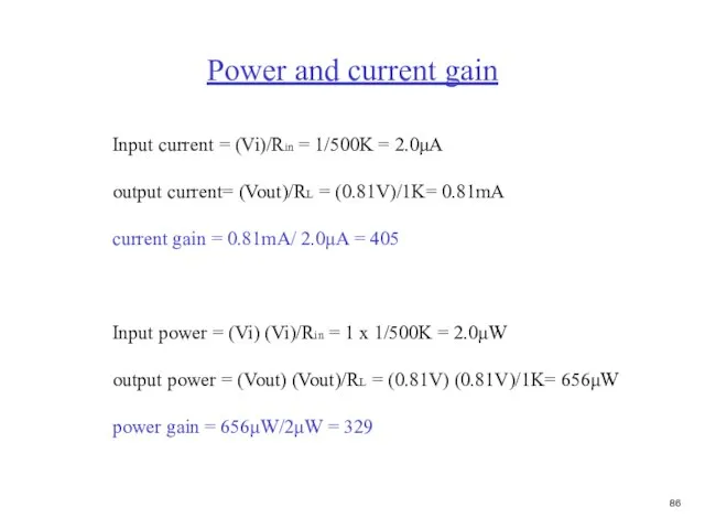
Слайд 87Power and current gain
Input current = (Vi)/Rin = 1/500K = 2.0μA
output current=
Power and current gain
Input current = (Vi)/Rin = 1/500K = 2.0μA
output current=
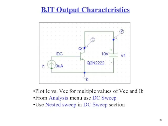
Слайд 88BJT Output Characteristics
Plot Ic vs. Vce for multiple values of Vce and
BJT Output Characteristics
Plot Ic vs. Vce for multiple values of Vce and
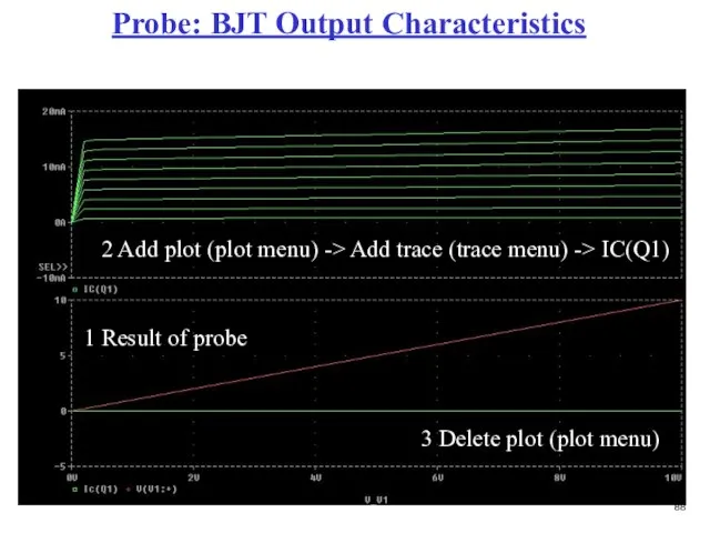
Слайд 89Probe: BJT Output Characteristics
1 Result of probe
2 Add plot (plot menu) ->
Probe: BJT Output Characteristics
1 Result of probe
2 Add plot (plot menu) ->
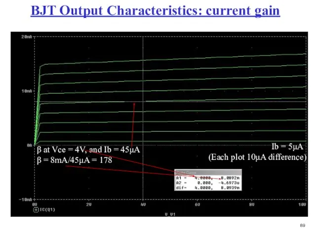
Слайд 90BJT Output Characteristics: current gain
Ib = 5μA
(Each plot 10μA difference)
β at Vce
BJT Output Characteristics: current gain
Ib = 5μA
(Each plot 10μA difference)
β at Vce
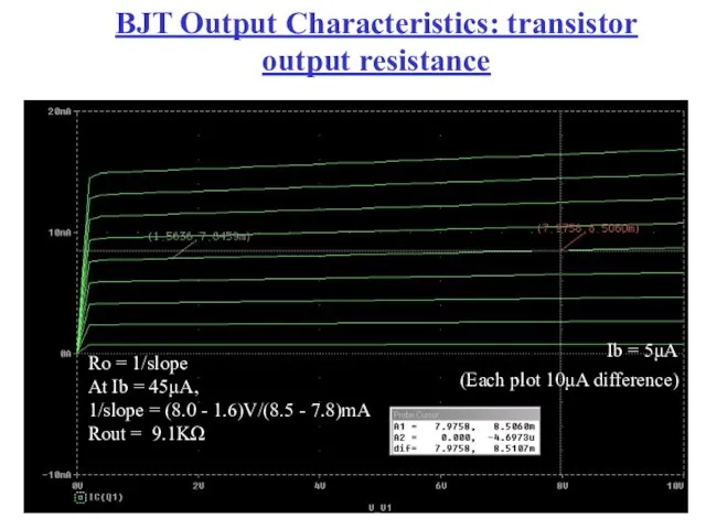
Слайд 91BJT Output Characteristics: transistor output resistance
Ib = 5μA
(Each plot 10μA difference)
Ro =
BJT Output Characteristics: transistor output resistance
Ib = 5μA
(Each plot 10μA difference)
Ro =
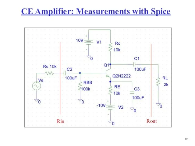
Слайд 92CE Amplifier: Measurements with Spice
Rin
Rout
CE Amplifier: Measurements with Spice
Rin
Rout
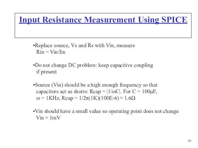
Слайд 93Input Resistance Measurement Using SPICE
Replace source, Vs and Rs with Vin, measure
Input Resistance Measurement Using SPICE
Replace source, Vs and Rs with Vin, measure
Слайд 94Rin Measurement
Transient analysis
Rin Measurement
Transient analysis
Слайд 95Probe results
I(C2)
Rin = 1mV/204nA
= 4.9KΩ
Probe results
I(C2)
Rin = 1mV/204nA
= 4.9KΩ
Слайд 96Output Resistance Measurement Using SPICE
Replace load, RL with Vin, measure Rin =
Output Resistance Measurement Using SPICE
Replace load, RL with Vin, measure Rin =
Слайд 97Rout Measurement
Transient analysis
Rout Measurement
Transient analysis
Слайд 98Probe results
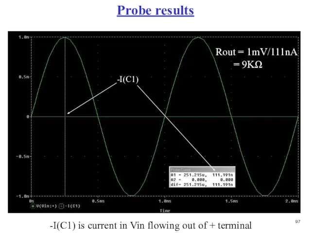
-I(C1)
Rout = 1mV/111nA
= 9KΩ
-I(C1) is current in Vin flowing out
Probe results
-I(C1)
Rout = 1mV/111nA
= 9KΩ
-I(C1) is current in Vin flowing out
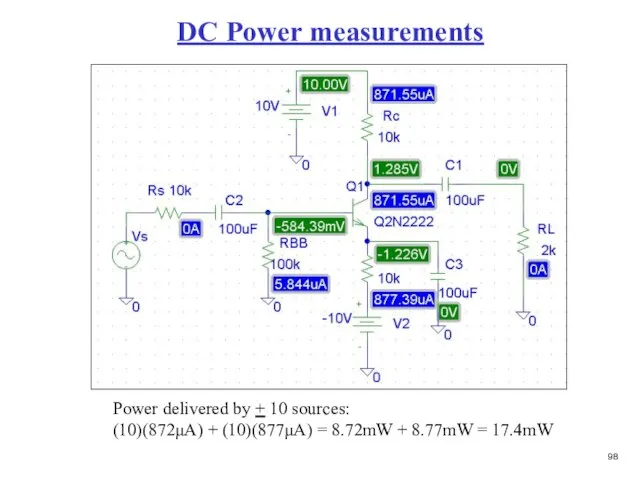
Слайд 99DC Power measurements
Power delivered by + 10 sources:
(10)(872μA) + (10)(877μA) =
DC Power measurements
Power delivered by + 10 sources:
(10)(872μA) + (10)(877μA) =
 Игры. Машинки
 Клуб сравнительного правоведения МГИМО
 Пропорции для срисовки
 РОЛЬ СЛОГАНА В РЕКЛАМЕ Атясова Анастасия, 2010 г.
 Фотоальбом. Целостность коллекции
 БИОХИМИЯ ПЕЧЕНИ
  Russkiy
 Лексикология – раздел науки о языке, в котором изучается слово
 Социальные проблемы современной реабилитации
 Архитектура распределённой системы
 Обобщение по теме Многочлены и одночлены
 Характер (от греч. charakter – печать, чеканка)
 Производительность комплекса систем
 Общероссийская общественная организация Всероссийская Организация Интллектуальной Собственности Общество по коллективному
 Скромник (SCP-096)
 Психолого-педагогическая готовность ребёнка к обучению в гимназии
 Projekt Aktywizacji Seniorów
 Стадии табачной эпидемии и смертность от табака
 Система Галактика ERP
 Выставка работ
 Закон и власть
  Квест-игра Почему нужно питаться правильно?
 Сергей Рахманинов. Фотография с дарственной надписью
 Выборочное федеральное наблюдение за затратами на производство и (или) реализацию товаров (работ, услуг) и результатами деятельнос
 Информационно-образовательная среда образовательного учреждения
 Достопримечательности Москвы
 Внедрение комплексной системы анализа, контроля, управления и предупреждения срыва сроков исполнения задач
 Братья наши меньшие.