- Deposition of Silicon Nitrides

Содержание
- 2. * Deposition of Silicon Nitrides Stoichiometric silicon nitride (Si3N4) is deposited at atmospheric pressure by reacting
- 3. * Deposition of Silicon Nitrides CVD and LPCVD silicon nitride films generally exhibit large tensile stresses
- 4. * Deposition of Silicon Nitrides For deposition below 400ºC, nonstoichiometric silicon nitride (SixNy) is obtained by
- 5. * Deposition of Silicon Nitrides A high value in the range is indicative of excess silicon,
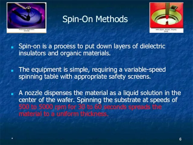
- 6. * Spin-On Methods Spin-on is a process to put down layers of dielectric insulators and organic
- 7. * Photoresists and polyimides are common organic materials that can be spun on a wafer with
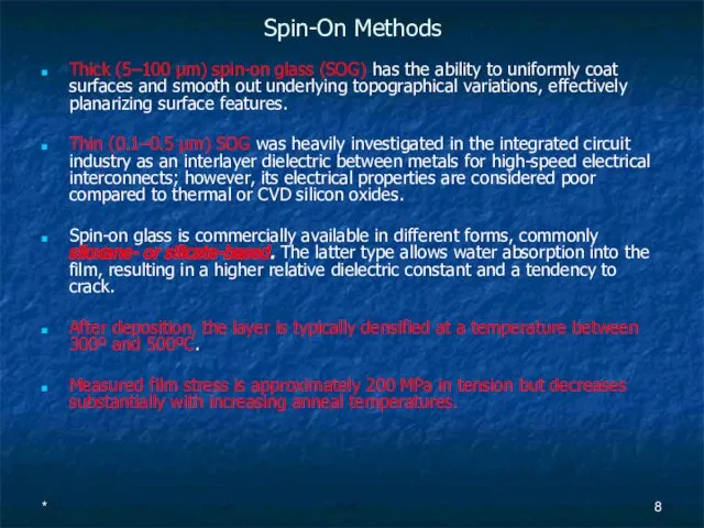
- 8. * Spin-On Methods Thick (5–100 µm) spin-on glass (SOG) has the ability to uniformly coat surfaces
- 9. * There are two basic types of SOG: siloxane-based organic SOG and silicate-based inorganic SOG. Spin
- 10. * A siloxane A siloxane is any chemical compound composed of units of the form R2SiSiOSiO,
- 11. * Silicate-based SOG
- 12. * Lithography The mask itself consists of a patterned opaque chromium (the most common), emulsion, or
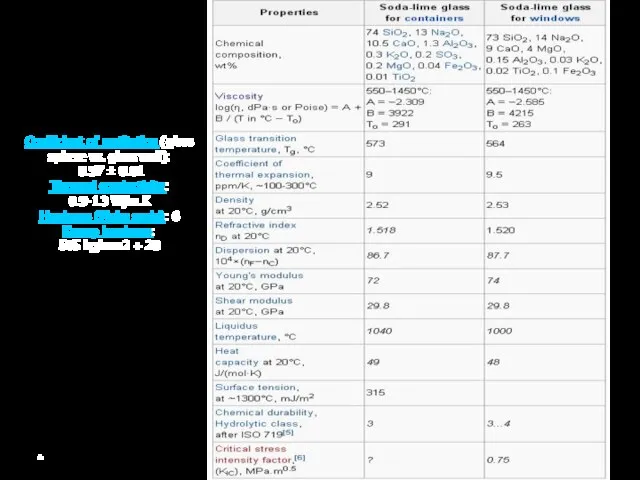
- 13. * Soda-lime glass Soda-lime glass, also called soda-lime-silica glass, is the most prevalent type of glass,
- 14. Soda-lime glass is divided technically into glass used for windows, called flat glass, and glass for
- 15. * Coefficient of restitution (glass sphere vs. glass wall): 0.97 ± 0.01 Thermal conductivity: 0.9-1.3 W/m.K
- 16. * Lime is a general term for calcium is a general term for calcium-containing inorganic materials
- 17. * Lithography Positive photoresist is an organic resin material containing a sensitizer. It is spin-coated on
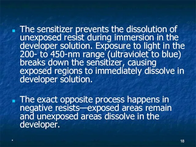
- 18. The sensitizer prevents the dissolution of unexposed resist during immersion in the developer solution. Exposure to
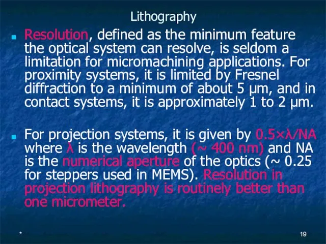
- 19. * Lithography Resolution, defined as the minimum feature the optical system can resolve, is seldom a
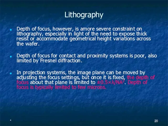
- 20. * Lithography Depth of focus, however, is amore severe constraint on lithography, especially in light of
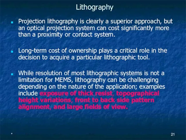
- 21. * Projection lithography is clearly a superior approach, but an optical projection system can cost significantly
- 22. * Thick Resist Patterned thick resist is normally used as a protective masking layer for the
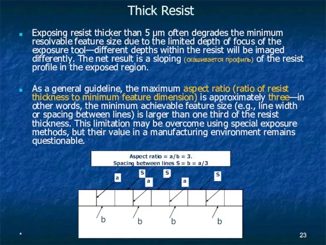
- 23. * Thick Resist Exposing resist thicker than 5 µm often degrades the minimum resolvable feature size
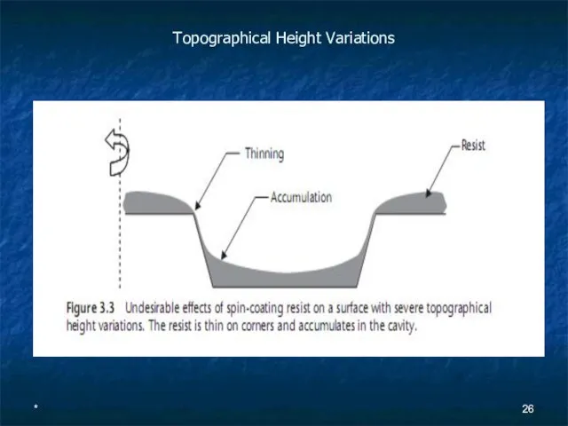
- 24. * Topographical Height Variations Changes in topography on the surface of the wafer, such as deep
- 25. * Topographical Height Variations Exposing a pattern on a surface with height variations in excess of
- 26. * Topographical Height Variations
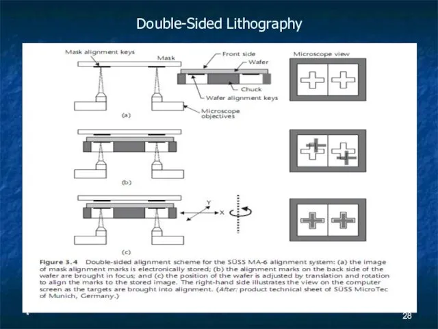
- 27. * Double-Sided Lithography Often, lithographic patterns on both sides of a wafer need to be aligned
- 28. * Double-Sided Lithography
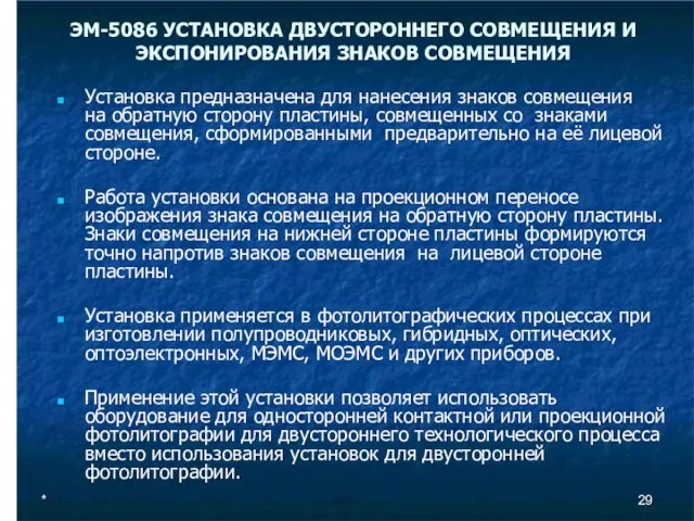
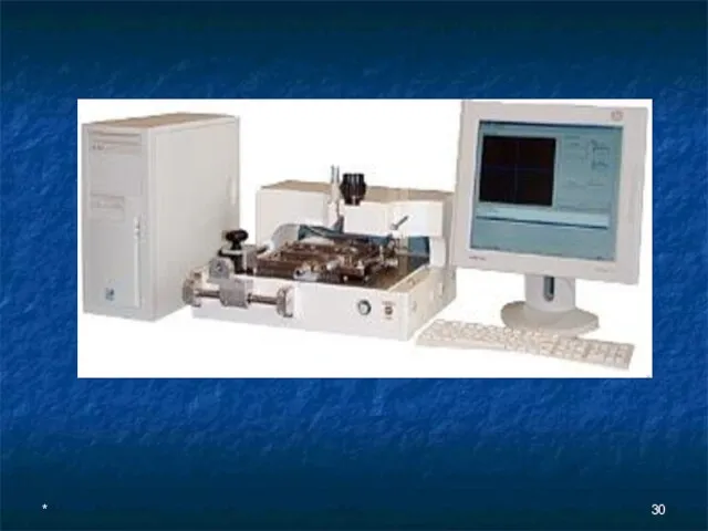
- 29. * ЭМ-5086 УСТАНОВКА ДВУСТОРОННЕГО СОВМЕЩЕНИЯ И ЭКСПОНИРОВАНИЯ ЗНАКОВ СОВМЕЩЕНИЯ Установка предназначена для нанесения знаков совмещения на
- 30. *
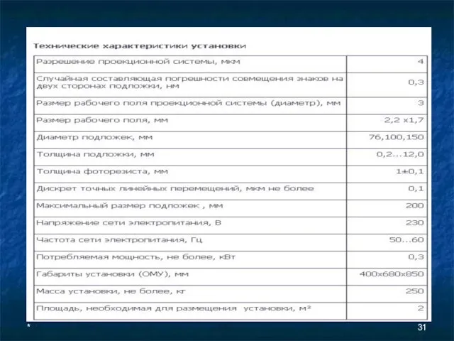
- 31. *
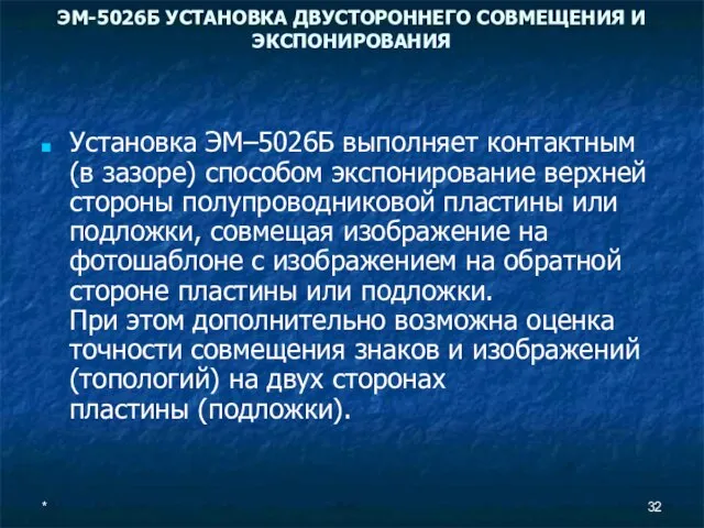
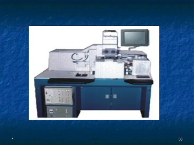
- 32. * ЭМ-5026Б УСТАНОВКА ДВУСТОРОННЕГО СОВМЕЩЕНИЯ И ЭКСПОНИРОВАНИЯ Установка ЭМ–5026Б выполняет контактным (в зазоре) способом экспонирование верхней
- 33. *
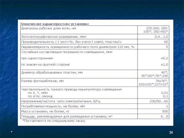
- 34. *
- 35. * Large Field of View (Большая область экспонирования) The field of view is the extent of
- 36. * In projection systems, the field of view is often less than 1 × 1cm2. The
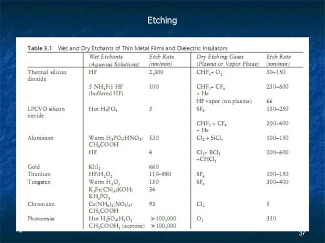
- 37. * Etching
- 38. * Оборудование фирмы SCR (Чехия) участка химического травления кремниевых пластин
- 39. * Isotropic Wet Etching The most common group of silicon isotropic wet etchants is HNA, also
- 40. * Isotropic and Anisotropic Etching
- 41. * Anisotropic wet etchants Anisotropic wet etchants are also known as orientation-dependent etchants (ODEs) because their
- 42. * Anisotropic Wet Etching
- 43. * KOH is by far the most common ODE Etch rates are typically given in the
- 45. Скачать презентацию
Слайд 2*
Deposition of Silicon Nitrides
Stoichiometric silicon nitride (Si3N4) is deposited at atmospheric pressure
*
Deposition of Silicon Nitrides
Stoichiometric silicon nitride (Si3N4) is deposited at atmospheric pressure
Слайд 3*
Deposition of Silicon Nitrides
CVD and LPCVD silicon nitride films generally exhibit large
*
Deposition of Silicon Nitrides
CVD and LPCVD silicon nitride films generally exhibit large
Слайд 4*
Deposition of Silicon Nitrides
For deposition below 400ºC, nonstoichiometric silicon nitride (SixNy) is
*
Deposition of Silicon Nitrides
For deposition below 400ºC, nonstoichiometric silicon nitride (SixNy) is
Слайд 5*
Deposition of Silicon Nitrides
A high value in the range is indicative of
*
Deposition of Silicon Nitrides
A high value in the range is indicative of
Слайд 6*
Spin-On Methods
Spin-on is a process to put down layers of dielectric insulators
*
Spin-On Methods
Spin-on is a process to put down layers of dielectric insulators
Слайд 7*
Photoresists and polyimides are common organic materials that can be spun on
*
Photoresists and polyimides are common organic materials that can be spun on
Слайд 8*
Spin-On Methods
Thick (5–100 µm) spin-on glass (SOG) has the ability to uniformly
*
Spin-On Methods
Thick (5–100 µm) spin-on glass (SOG) has the ability to uniformly
Слайд 9*
There are two basic types of SOG: siloxane-based organic SOG and silicate-based
*
There are two basic types of SOG: siloxane-based organic SOG and silicate-based
Слайд 10*
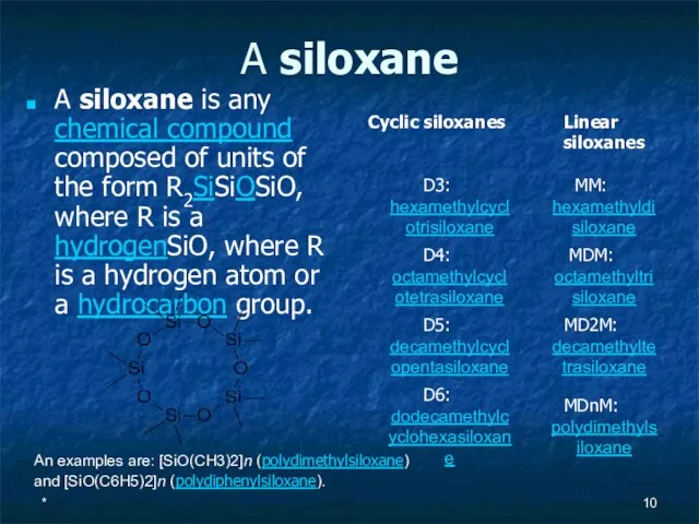
A siloxane
A siloxane is any chemical compound composed of units of the
*
A siloxane
A siloxane is any chemical compound composed of units of the
Слайд 11*
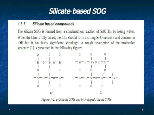
Silicate-based SOG
*
Silicate-based SOG
Слайд 12*
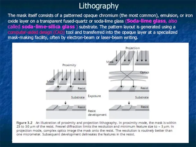
Lithography
The mask itself consists of a patterned opaque chromium (the most common),
*
Lithography
The mask itself consists of a patterned opaque chromium (the most common),
Слайд 13*
Soda-lime glass
Soda-lime glass, also called soda-lime-silica glass, is the most prevalent type of glass,
*
Soda-lime glass
Soda-lime glass, also called soda-lime-silica glass, is the most prevalent type of glass,
Слайд 14Soda-lime glass is divided technically into glass used for windows, called flat glass,
Soda-lime glass is divided technically into glass used for windows, called flat glass,
Слайд 15*
Coefficient of restitution (glass sphere vs. glass wall):
0.97 ± 0.01
Thermal conductivity:
0.9-1.3
*
Coefficient of restitution (glass sphere vs. glass wall):
0.97 ± 0.01
Thermal conductivity:
0.9-1.3
Слайд 16*
Lime is a general term for calcium is a general term for calcium-containing inorganic materials
Lime is a general term
*
Lime is a general term for calcium is a general term for calcium-containing inorganic materials
Lime is a general term
Слайд 17*
Lithography
Positive photoresist is an organic resin material containing a sensitizer. It is
*
Lithography
Positive photoresist is an organic resin material containing a sensitizer. It is
Слайд 18The sensitizer prevents the dissolution of unexposed resist during immersion in the
The sensitizer prevents the dissolution of unexposed resist during immersion in the
Слайд 19*
Lithography
Resolution, defined as the minimum feature the optical system can resolve, is
*
Lithography
Resolution, defined as the minimum feature the optical system can resolve, is
Слайд 20*
Lithography
Depth of focus, however, is amore severe constraint on lithography, especially in
*
Lithography
Depth of focus, however, is amore severe constraint on lithography, especially in
Слайд 21*
Projection lithography is clearly a superior approach, but an optical projection system
*
Projection lithography is clearly a superior approach, but an optical projection system
Слайд 22*
Thick Resist
Patterned thick resist is normally used as a protective masking layer
*
Thick Resist
Patterned thick resist is normally used as a protective masking layer
Слайд 23*
Thick Resist
Exposing resist thicker than 5 µm often degrades the minimum resolvable
*
Thick Resist
Exposing resist thicker than 5 µm often degrades the minimum resolvable
Слайд 24*
Topographical Height Variations
Changes in topography on the surface of the wafer, such
*
Topographical Height Variations
Changes in topography on the surface of the wafer, such
Слайд 25*
Topographical Height Variations
Exposing a pattern on a surface with height variations in
*
Topographical Height Variations
Exposing a pattern on a surface with height variations in
Слайд 26*
Topographical Height Variations
*
Topographical Height Variations
Слайд 27*
Double-Sided Lithography
Often, lithographic patterns on both sides of a wafer need to
*
Double-Sided Lithography
Often, lithographic patterns on both sides of a wafer need to
Слайд 28*
Double-Sided Lithography
*
Double-Sided Lithography
Слайд 29*
ЭМ-5086 УСТАНОВКА ДВУСТОРОННЕГО СОВМЕЩЕНИЯ И ЭКСПОНИРОВАНИЯ ЗНАКОВ СОВМЕЩЕНИЯ
Установка предназначена для нанесения знаков
*
ЭМ-5086 УСТАНОВКА ДВУСТОРОННЕГО СОВМЕЩЕНИЯ И ЭКСПОНИРОВАНИЯ ЗНАКОВ СОВМЕЩЕНИЯ
Установка предназначена для нанесения знаков
Слайд 32*
ЭМ-5026Б УСТАНОВКА ДВУСТОРОННЕГО СОВМЕЩЕНИЯ И ЭКСПОНИРОВАНИЯ
Установка ЭМ–5026Б выполняет контактным (в зазоре) способом
*
ЭМ-5026Б УСТАНОВКА ДВУСТОРОННЕГО СОВМЕЩЕНИЯ И ЭКСПОНИРОВАНИЯ
Установка ЭМ–5026Б выполняет контактным (в зазоре) способом
Слайд 35*
Large Field of View (Большая область экспонирования)
The field of view is the
*
Large Field of View (Большая область экспонирования)
The field of view is the
Слайд 36*
In projection systems, the field of view is often less than 1
*
In projection systems, the field of view is often less than 1
Слайд 37*
Etching
*
Etching
Слайд 38*
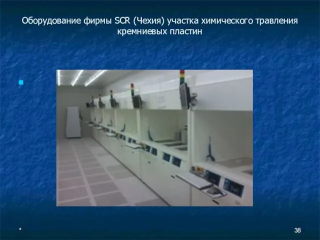
Оборудование фирмы SCR (Чехия) участка химического травления кремниевых пластин
*
Оборудование фирмы SCR (Чехия) участка химического травления кремниевых пластин
Слайд 39*
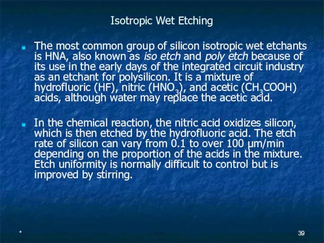
Isotropic Wet Etching
The most common group of silicon isotropic wet etchants is
*
Isotropic Wet Etching
The most common group of silicon isotropic wet etchants is
Слайд 40*
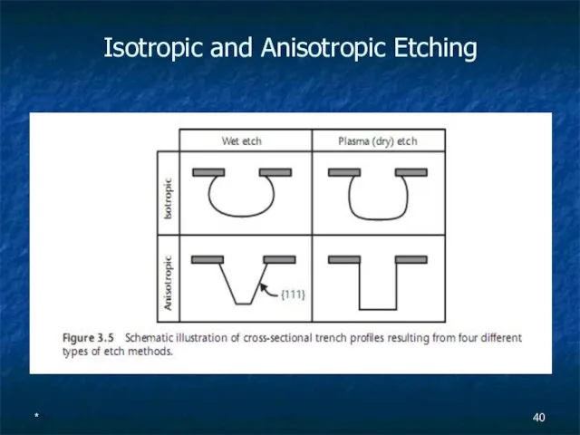
Isotropic and Anisotropic Etching
*
Isotropic and Anisotropic Etching
Слайд 41*
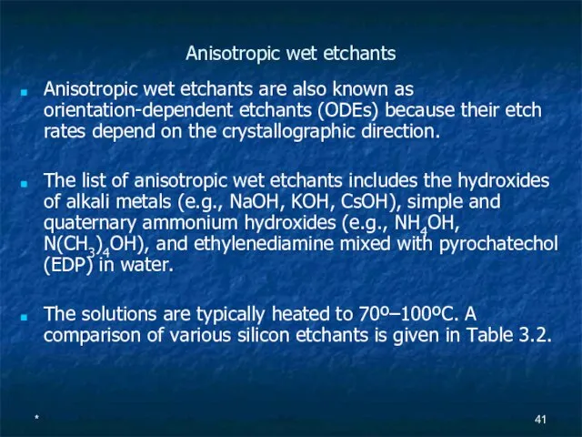
Anisotropic wet etchants
Anisotropic wet etchants are also known as orientation-dependent etchants (ODEs)
*
Anisotropic wet etchants
Anisotropic wet etchants are also known as orientation-dependent etchants (ODEs)
Слайд 42*
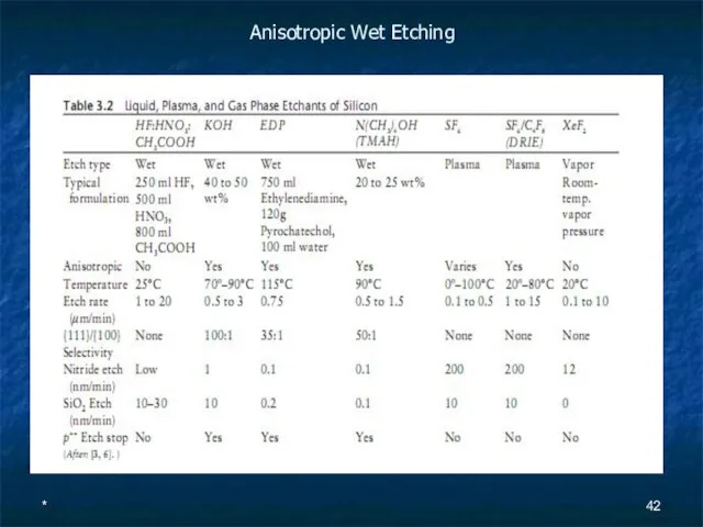
Anisotropic Wet Etching
*
Anisotropic Wet Etching
Слайд 43*
KOH is by far the most common ODE
Etch rates are typically given
*
KOH is by far the most common ODE
Etch rates are typically given
 Презентация на тему Мой город
 Аудитория Интернета
 www.spbmapo.ru
 Экологические проекты должны стать обязательной составной частью программы развития каждого моногорода
 Модели психологического воздействия в рекламе
 Sano karjalakse
 Автоматизированная информационная система управления кадрами предприятия «Кадры-Домино»
 Лаборатория манипуляции. 10 тайных уязвимостей
 Ляйсан. Налог на имущество физических лиц
 Ветеринарная аптека
 Развитие семейных форм устройства детей-сирот и детей, оставшихся без попечения родителей, в Республике Карелия
 Образование и культура в XVII веке
 Лесков
 Итоговое сочинение. Рекомендации
 Презентация на тему Экологическое воспитание детей через сказку
  Типы химической связи
 Часы в живописи
 Презентация на тему Рассказ - Весна
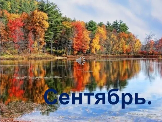 Презентация на тему Сентябрь
  Отражение. Синопсис
 Общая физиология ЦНС и возбудимых тканей
 Способы преобразования положения фигуры относительно плоскостей проекций
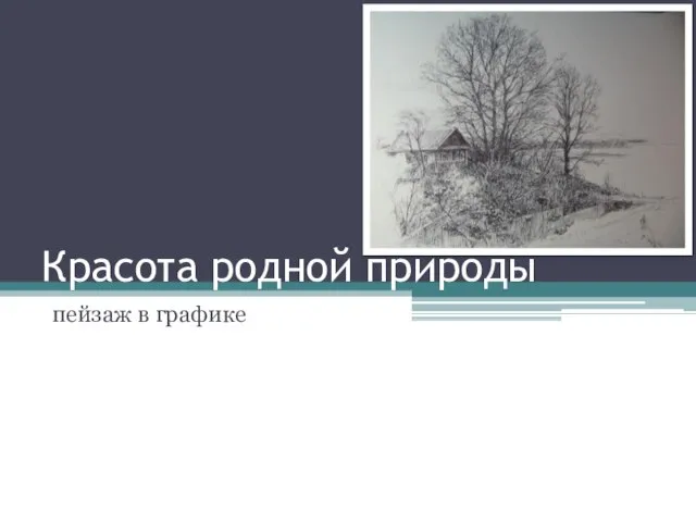 Красота родной природы пейзаж в графике
 Маска = защита + индивидуальность
 Политическое сознание
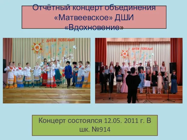 Отчётный концерт объединения «Матвеевское» ДШИ «Вдохновение»
 Program Manager Individual Combat Equipment (ICE) Marine Corps
 3U-кубсат и его применение