- Material Aspects of Micro- and Nanoelectromechanical

Содержание
- 2. 08/11/2023 Two of the more significant technological achievements during the last 30 years have been the
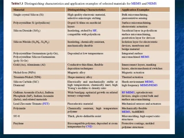
- 3. 08/11/2023 A well-rounded understanding of MEMS and NEMS requires a basic knowledge of the materials used
- 4. 08/11/2023
- 5. 08/11/2023
- 6. 08/11/2023 1. Single Crystal Silicon Single crystal Si is material for bulk and surface micromachining, due
- 7. 08/11/2023 Bulk micromachining is a process whereby etching techniques are used in conjunction with etch masks
- 8. 08/11/2023 In contrast to anisotropic etching, isotropic etching exhibits no selectivity to the various crystal planes.
- 9. 08/11/2023 Boron-doped etch stops are often less than 10µm thick, since the boron concentration in Si
- 10. 08/11/2023 Dry etching processes are available to pattern single crystal Si. The process spectrum ranges from
- 11. 08/11/2023 The RIE process is highly directional, which enables direct pattern transfer from an overlying masking
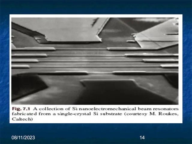
- 12. 08/11/2023 A wide variety of microfabricated devices have been made from single crystal Si, such as
- 13. 08/11/2023 By coupling electron-beam (e-beam) lithography with conventional Si etching, device structures with submicron dimensions have
- 14. 08/11/2023
- 15. 08/11/2023 In-plane nanoelectromechanical resonators based on silicon nanowire piezoresistive detection E Mile*, G Jourdan*, I Bargatin
- 16. 08/11/2023 In-plane nanoelectromechanical resonators based on silicon nanowire piezoresistive detection The NEMS device presented in this
- 17. 08/11/2023 The top silicon layer was implanted with boron ions (p-type) through a thin layer of
- 18. 08/11/2023 A hybrid e-beam/DUV lithography technique (allowing 50 nm minimum feature size) was used to define
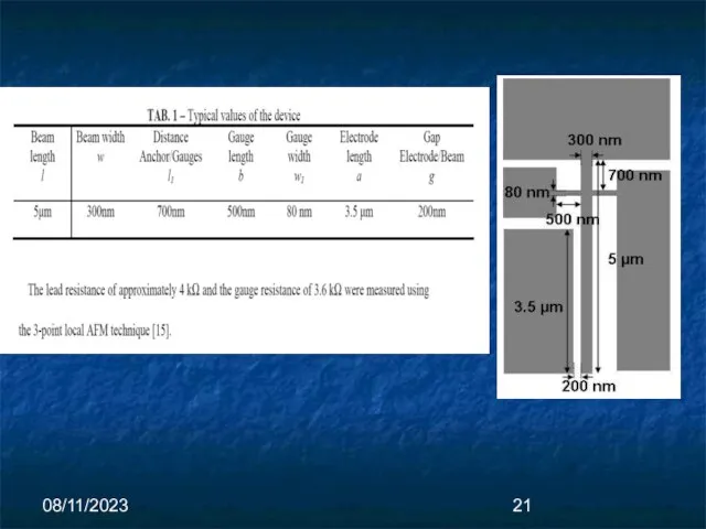
- 19. 08/11/2023 The NEMS is composed of a fixed-free lever beam and two piezoresistive gauges connected to
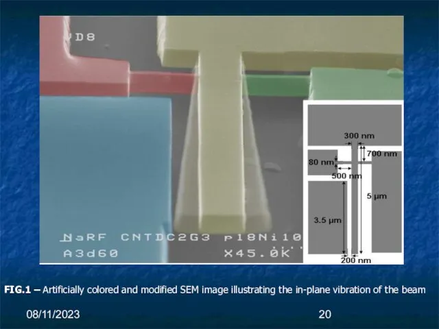
- 20. 08/11/2023 FIG.1 – Artificially colored and modified SEM image illustrating the in-plane vibration of the beam
- 21. 08/11/2023
- 22. 08/11/2023 Silicon as an element exists with three different microstructures: crystalline, polycrystalline, or amorphous. Polycrystalline, or
- 23. 08/11/2023 Standard 100-mm wafers are nominally 525 µm thick, and 150-mm wafers are typically 650 µm
- 24. 08/11/2023
- 25. 08/11/2023 Silicon is a very good thermal conductor with a thermal conductivity greater than that of
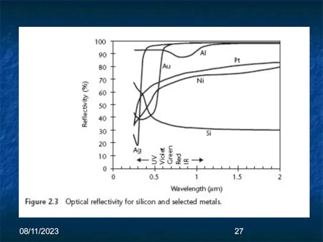
- 26. 08/11/2023 Unfortunately, silicon is not an active optical material—silicon-based lasers do not exist. Because of the
- 27. 08/11/2023
- 28. 08/11/2023 Silicon is also well known to retain its mechanical integrity at temperatures up to about
- 29. 08/11/2023 The interactions of silicon with gases, chemicals, biological fluids, and enzymes (ферменты) remain the subject
- 30. 08/11/2023 In medicine and biology, studies are ongoing to evaluate silicon for medical implants. Preliminary medical
- 31. 08/11/2023
- 32. 08/11/2023 Polysilicon Surface micromachining is a process whereby a sequence of thin films, often of different
- 33. 08/11/2023 Like single crystal Si, polysilicon can be doped during or after film deposition. SiO2 can
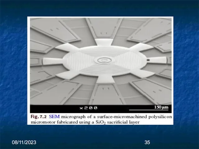
- 34. 08/11/2023 SiO2 is readily dissolvable in hydrofluoric acid (HF), which does not etch polysilicon and, thus,
- 35. 08/11/2023
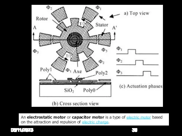
- 36. 08/11/2023 An electrostatic motor or capacitor motor is a type of electric motor based on the
- 37. 08/11/2023 For MEMS and IC applications, polysilicon films are commonly deposited using a process known as
- 38. 08/11/2023 Polysilicon thin films consist of a collection of small single crystal grains whose microstructure and
- 39. 08/11/2023 In terms of chemical resistance, polysilicon is very much like single crystal Si. The oxidation
- 40. 08/11/2023 Diffusion is an effective method for doping polysilicon films, especially for heavy doping of thick
- 41. 08/11/2023 Ion implantation is also used to dope polysilicon films. A high-temperature annealing step is usually
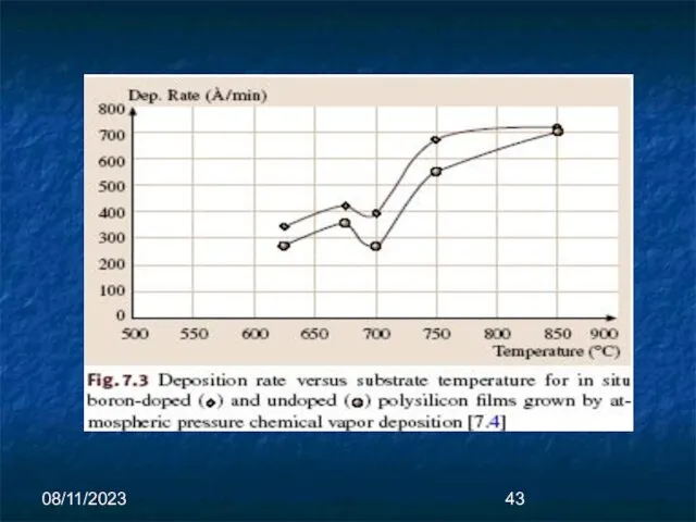
- 42. 08/11/2023 The addition of dopants during the deposition process not only modifies the conductivity, but also
- 43. 08/11/2023
- 44. 08/11/2023 Although commonly used to produce doped polysilicon for electrostatic devices, Cao et al. have used
- 45. 08/11/2023 For thick films with large grains, the thermal conductivity ranges between 50% and 85% of
- 46. 08/11/2023 Annealing can be used to reduce the compressive stress in as-deposited polysilicon films. For instance,
- 47. 08/11/2023 Zhang et al. reported that a 10 s anneal at 1,100 ◦C was sufficient to
- 48. 08/11/2023 As an alternative to high-temperature annealing, Yang et al. have developed an approach that actually
- 49. 08/11/2023 The tensile layers consist of fine-grained polysilicon grown at a temperature of 570 ◦C, while
- 50. 08/11/2023 The process achieves stress reduction reduction without high-temperature annealing, a considerable advantage for integrated MEMS
- 51. 08/11/2023 Unlike conventional LPCVD processes with deposition rates of less than 100A/min, epitaxial processes have deposition
- 52. 08/11/2023 An LPCVD polysilicon seed layer is sometimes used to control nucleation, grain size, and surface
- 53. 08/11/2023 Compressive films generally have a mixture of [110] and [311] grains, while tensile films have
- 54. 08/11/2023 All of the aforementioned (вышеупомянутые) polysilicon deposition processes utilize substrate temperatures in excess (превышение) of
- 55. 08/11/2023 The process involved DC magnitron sputtering from a Si target using an Ar sputtering gas,
- 57. Скачать презентацию
Слайд 308/11/2023
A well-rounded understanding of MEMS and NEMS requires a basic knowledge of
08/11/2023
A well-rounded understanding of MEMS and NEMS requires a basic knowledge of
Слайд 408/11/2023
08/11/2023
Слайд 508/11/2023
08/11/2023
Слайд 608/11/2023
1. Single Crystal Silicon
Single crystal Si is material for bulk and
08/11/2023
1. Single Crystal Silicon
Single crystal Si is material for bulk and
Слайд 708/11/2023
Bulk micromachining is a process whereby etching techniques are used in conjunction
08/11/2023
Bulk micromachining is a process whereby etching techniques are used in conjunction
Слайд 808/11/2023
In contrast to anisotropic etching, isotropic etching exhibits no selectivity to the
08/11/2023
In contrast to anisotropic etching, isotropic etching exhibits no selectivity to the
Слайд 908/11/2023
Boron-doped etch stops are often less than 10µm thick, since the boron
08/11/2023
Boron-doped etch stops are often less than 10µm thick, since the boron
Слайд 1008/11/2023
Dry etching processes are available to pattern single crystal Si. The process
08/11/2023
Dry etching processes are available to pattern single crystal Si. The process
Слайд 1108/11/2023
The RIE process is highly directional, which enables direct pattern transfer from
08/11/2023
The RIE process is highly directional, which enables direct pattern transfer from
Слайд 1208/11/2023
A wide variety of microfabricated devices have been made from single crystal
08/11/2023
A wide variety of microfabricated devices have been made from single crystal
Слайд 1308/11/2023
By coupling electron-beam (e-beam) lithography with conventional Si etching, device structures with
08/11/2023
By coupling electron-beam (e-beam) lithography with conventional Si etching, device structures with
Слайд 1408/11/2023
08/11/2023
Слайд 1508/11/2023
In-plane nanoelectromechanical resonators based on silicon nanowire
piezoresistive detection
E Mile*, G Jourdan*, I
08/11/2023
In-plane nanoelectromechanical resonators based on silicon nanowire
piezoresistive detection
E Mile*, G Jourdan*, I
Слайд 1608/11/2023
In-plane nanoelectromechanical resonators based on silicon nanowire piezoresistive detection
The NEMS device presented
08/11/2023
In-plane nanoelectromechanical resonators based on silicon nanowire piezoresistive detection
The NEMS device presented
Слайд 1708/11/2023
The top silicon layer was implanted with boron ions (p-type) through a
08/11/2023
The top silicon layer was implanted with boron ions (p-type) through a
Слайд 1808/11/2023
A hybrid e-beam/DUV lithography technique (allowing 50 nm minimum feature size) was
08/11/2023
A hybrid e-beam/DUV lithography technique (allowing 50 nm minimum feature size) was
Слайд 1908/11/2023
The NEMS is composed of a fixed-free lever beam and two piezoresistive
08/11/2023
The NEMS is composed of a fixed-free lever beam and two piezoresistive
Слайд 2008/11/2023
FIG.1 – Artificially colored and modified SEM image illustrating the in-plane vibration
08/11/2023
FIG.1 – Artificially colored and modified SEM image illustrating the in-plane vibration
Слайд 2108/11/2023
08/11/2023
Слайд 2208/11/2023
Silicon as an element exists with three different microstructures: crystalline, polycrystalline, or
08/11/2023
Silicon as an element exists with three different microstructures: crystalline, polycrystalline, or
Слайд 2308/11/2023
Standard 100-mm wafers are nominally 525 µm thick, and 150-mm wafers are
08/11/2023
Standard 100-mm wafers are nominally 525 µm thick, and 150-mm wafers are
Слайд 2408/11/2023
08/11/2023
Слайд 2508/11/2023
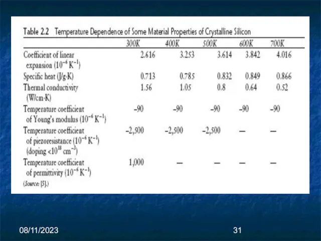
Silicon is a very good thermal conductor with a thermal conductivity greater
08/11/2023
Silicon is a very good thermal conductor with a thermal conductivity greater
Слайд 2608/11/2023
Unfortunately, silicon is not an active optical material—silicon-based lasers do not exist.
08/11/2023
Unfortunately, silicon is not an active optical material—silicon-based lasers do not exist.
Слайд 2708/11/2023
08/11/2023
Слайд 2808/11/2023
Silicon is also well known to retain its mechanical integrity at temperatures
08/11/2023
Silicon is also well known to retain its mechanical integrity at temperatures
Слайд 2908/11/2023
The interactions of silicon with gases, chemicals, biological fluids, and enzymes (ферменты)
08/11/2023
The interactions of silicon with gases, chemicals, biological fluids, and enzymes (ферменты)
Слайд 3008/11/2023
In medicine and biology, studies are ongoing to evaluate silicon for medical
08/11/2023
In medicine and biology, studies are ongoing to evaluate silicon for medical
Слайд 3108/11/2023
08/11/2023
Слайд 3208/11/2023
Polysilicon
Surface micromachining is a process whereby a sequence of thin films, often
08/11/2023
Polysilicon
Surface micromachining is a process whereby a sequence of thin films, often
Слайд 3308/11/2023
Like single crystal Si, polysilicon can be doped during or after film
08/11/2023
Like single crystal Si, polysilicon can be doped during or after film
Слайд 3408/11/2023
SiO2 is readily dissolvable in hydrofluoric acid (HF), which does not etch
08/11/2023
SiO2 is readily dissolvable in hydrofluoric acid (HF), which does not etch
Слайд 3508/11/2023
08/11/2023
Слайд 3608/11/2023
An electrostatic motor or capacitor motor is a type of electric motor based on the attraction and repulsion
08/11/2023
An electrostatic motor or capacitor motor is a type of electric motor based on the attraction and repulsion
Слайд 3708/11/2023
For MEMS and IC applications, polysilicon films are commonly deposited using a
08/11/2023
For MEMS and IC applications, polysilicon films are commonly deposited using a
Слайд 3808/11/2023
Polysilicon thin films consist of a collection of small single crystal grains
08/11/2023
Polysilicon thin films consist of a collection of small single crystal grains
Слайд 3908/11/2023
In terms of chemical resistance, polysilicon is very much like single crystal
08/11/2023
In terms of chemical resistance, polysilicon is very much like single crystal
Слайд 4008/11/2023
Diffusion is an effective method for doping polysilicon films, especially for heavy
08/11/2023
Diffusion is an effective method for doping polysilicon films, especially for heavy
Слайд 4108/11/2023
Ion implantation is also used to dope polysilicon films.
A high-temperature annealing
08/11/2023
Ion implantation is also used to dope polysilicon films.
A high-temperature annealing
Слайд 4208/11/2023
The addition of dopants during the deposition process not only modifies the
08/11/2023
The addition of dopants during the deposition process not only modifies the
Слайд 4308/11/2023
08/11/2023
Слайд 4408/11/2023
Although commonly used to produce doped polysilicon for electrostatic devices, Cao et
08/11/2023
Although commonly used to produce doped polysilicon for electrostatic devices, Cao et
Слайд 4508/11/2023
For thick films with large grains, the thermal conductivity ranges between 50%
08/11/2023
For thick films with large grains, the thermal conductivity ranges between 50%
Слайд 4608/11/2023
Annealing can be used to reduce the compressive stress in as-deposited polysilicon
08/11/2023
Annealing can be used to reduce the compressive stress in as-deposited polysilicon
Слайд 4708/11/2023
Zhang et al. reported that a 10 s anneal at 1,100 ◦C
08/11/2023
Zhang et al. reported that a 10 s anneal at 1,100 ◦C
Слайд 4808/11/2023
As an alternative to high-temperature annealing, Yang et al. have developed an
08/11/2023
As an alternative to high-temperature annealing, Yang et al. have developed an
Слайд 4908/11/2023
The tensile layers consist of fine-grained polysilicon grown at a temperature of
08/11/2023
The tensile layers consist of fine-grained polysilicon grown at a temperature of
Слайд 5008/11/2023
The process achieves stress reduction reduction without high-temperature annealing, a considerable advantage
08/11/2023
The process achieves stress reduction reduction without high-temperature annealing, a considerable advantage
Слайд 5108/11/2023
Unlike conventional LPCVD processes with deposition rates of less than 100A/min, epitaxial
08/11/2023
Unlike conventional LPCVD processes with deposition rates of less than 100A/min, epitaxial
Слайд 5208/11/2023
An LPCVD polysilicon seed layer is sometimes used to control nucleation, grain
08/11/2023
An LPCVD polysilicon seed layer is sometimes used to control nucleation, grain
Слайд 5308/11/2023
Compressive films generally have a mixture of [110] and [311] grains, while
08/11/2023
Compressive films generally have a mixture of [110] and [311] grains, while
![08/11/2023 Compressive films generally have a mixture of [110] and [311] grains,](/_ipx/f_webp&q_80&fit_contain&s_1440x1080/imagesDir/jpg/373534/slide-52.jpg)
Слайд 5408/11/2023
All of the aforementioned (вышеупомянутые) polysilicon deposition processes utilize substrate temperatures in
08/11/2023
All of the aforementioned (вышеупомянутые) polysilicon deposition processes utilize substrate temperatures in
Слайд 5508/11/2023
The process involved DC magnitron sputtering from a Si target using an
08/11/2023
The process involved DC magnitron sputtering from a Si target using an
 Презентация на тему Глобальное потепление
  Шкала электромагнитных излучений
 Нашествие с Востока на Русь
 Пример построения системы управления машиностроительным производством
 Государственная поддержка агрострахования и мелиорации земель
 2012 год. Цементный рынок: как жить в эпоху дефицита?
 ТЕМА: Пластик- удобно, выгодно, губительно!
 Технологическое нормирование эксплуатационной работы железных дорог
 Швидке читання - запорука успішного навчання
 Презентация на тему Франция
 МАФ из современных материалов для детских площадок
 Материалы для подготовки к контрольной работе по теме Греция
 Вредные привычки у детей. Консультация для родителей
 Анализ препятствий на пути расширения доступа к услугам по ДКТ и внедрения системы супервизии
 БИОГРАФИЯ Лавриненкова Владимира Дмитриевича Родился 15 Мая 1919 года в деревне Птахино, Смоленской области, в семье крестьянина. В 1
 Добыча полезных ископаемых на Луне из реголита
 Социальная политика государства
 20161109_prezentatsiya_1
 Презентация на тему Русской речи государь по прозванию Словарь
 Народная игрушка в развитии дошкольников
 Информационный поиск в Интернете
 Жисмоний шахс ер мулк соликлар
 Жанры изобразительного искусства
 Эффективное регулирование на конкурентных энергетических рынках обеспечивает доступность энергии Сергей Геннадьевич Новиков
  Презентация на тему Школа будущего
 Рисованные объекты Действия над объектами
 Система диагностики и коррекции как снятие психолого-педагогических трудностей при обучении математике слабоуспевающего учени
 Вместе мы – сила!